- 您現(xiàn)在的位置:買(mǎi)賣(mài)IC網(wǎng) > PDF目錄67762 > M35502AFP 7 X 18 SEGMENTS FLUORESCENT DSPL CTRL, PDSO36 PDF資料下載
參數(shù)資料
| 型號(hào): | M35502AFP |
| 元件分類(lèi): | 顯示控制器 |
| 英文描述: | 7 X 18 SEGMENTS FLUORESCENT DSPL CTRL, PDSO36 |
| 封裝: | 0.450 INCH, PLASTIC, SSOP-36 |
| 文件頁(yè)數(shù): | 1/16頁(yè) |
| 文件大?。?/td> | 218K |
| 代理商: | M35502AFP |
當(dāng)前第1頁(yè)第2頁(yè)第3頁(yè)第4頁(yè)第5頁(yè)第6頁(yè)第7頁(yè)第8頁(yè)第9頁(yè)第10頁(yè)第11頁(yè)第12頁(yè)第13頁(yè)第14頁(yè)第15頁(yè)第16頁(yè)
M35502AFP
DESCRIPTION/FEATURES
High-breakdown-voltage output port ......................................... 25
Segment output ............................................ 8 to 20
Digit output ................................................... 5 to 16
(Ports P0 to P2 are also used as normal output ports)
Output breakdown .................................. Vcc – 45 V
Output current ............... –18 mA (at DIG selecting),
–7 mA (at SEG selecting)
Pull-down resistor ......................................... built-in
Dimmer switch ............................................ 4 levels
A-D converter ................................................... 8-bit ! 4 channels
Absolute accuracy ....................................... ±3 LSB
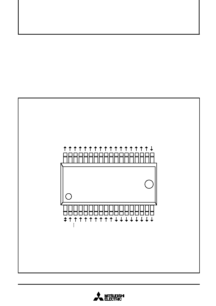
PIN CONFIGURATION (TOP VIEW)
MITSUBISHI LINEAR IC’s
FLD CONTROLLER
Serial I/O ..................................... 3 (CS controller, external clock)
Noise filter ..................................................... built-in
(in serial input pin and clock pin, 2 MHz sampling)
FLD display data ............................................. input
A-D conversion data ..................................... output
Command ....................................................... input
Package ......................................................................... 36P2R-G
Oscillation circuit ........... CR oscillation cirucit (external capacitor)
Oscillation frequency..................................... 2 MHz
Power source voltage .................................................. 4.0 to 5.5 V
Fig.1 Pin configuration of M35502AFP
Package type: 36P2R-G
FLD
0
FLD
1
FLD
2
FLD
3
FLD
4
FLD
5
FLD
6
FLD
7
FLD
8
FLD
9
FLD
10
FLD
11
FLD
12
FLD
13
FLD
14
FLD
FLD
16
V
EE
S
DATA
S
CLK
CS
AN
3
AN
2
AN
1
AN
0
V
SS
OSC
V
CC
FLD
24
/P0
FLD
23
/P1
FLD
22
/P2
FLD
21
FLD
20
FLD
19
FLD
18
FLD
17
1
2
3
4
5
6
7
8
9
10
11
12
13
14
15
16
17
18
36
35
34
33
32
31
30
29
28
27
26
25
24
23
22
21
20
19
M35502AFP
相關(guān)PDF資料 |
PDF描述 |
|---|---|
| M37150MC-XXXFP | 8-BIT, MROM, 8.95 MHz, MICROCONTROLLER, PDSO42 |
| M37150EFFP | 8-BIT, OTPROM, 8.95 MHz, MICROCONTROLLER, PDSO42 |
| M37150M8-XXXFP | 8-BIT, MROM, 8.95 MHz, MICROCONTROLLER, PDSO42 |
| M37150MA-XXXFP | 8-BIT, MROM, 8.95 MHz, MICROCONTROLLER, PDSO42 |
| M37151M8-XXXFP | 8-BIT, MROM, 8.1 MHz, MICROCONTROLLER, PDSO42 |
相關(guān)代理商/技術(shù)參數(shù) |
參數(shù)描述 |
|---|---|
| M3554 | 制造商:Baldor Electric Company 功能描述: |
| M3558 | 制造商:BALDOR MOTORS 功能描述: 制造商:Baldor Electric Company 功能描述: |
| M3558T | 制造商:BALDOR MOTORS 功能描述: |
| M3560-B | 制造商:RAF Electronic Hardware 功能描述:Metric Round Thumb Nuts |
| M3560-B-12 | 功能描述:安裝硬件 Rnd Thumb Nut BCZ M2.5X0.45 6mm RoHS:否 制造商:Harwin 類(lèi)型:SMT Cable Clip 材料:Phosphor Bronze 安裝孔大小: 長(zhǎng)度:5 mm 外徑: 內(nèi)徑: 厚度: 電鍍:Tin 螺紋大小: |
發(fā)布緊急采購(gòu),3分鐘左右您將得到回復(fù)。