- 您現(xiàn)在的位置:買賣IC網(wǎng) > PDF目錄370839 > M35501BGP (Mitsubishi Electric Corporation) FLD ( VFD) Controller(真空熒光顯示器控制器) PDF資料下載
參數(shù)資料
12
MITSUBISHI <DIGITAL ASSP>
M35500AFP/BGP
FLD(VFD) CONTROLLER
t
w(RESET)
t
c
(X
IN
)
t
wH
(X
IN
)
t
wL
(X
IN
)
t
c
(S
CLK
)
t
wH
(S
CLK
)
t
wL
(S
CLK
)
t
su
(S
IN
-S
CLK
)
t
h
(S
CLK
-S
IN
)
t
su
(CS)
t
h
(CS)
t
re
(S
CLK
)
t
d
(S
CLK
-S
OUT
)
t
v
(S
CLK
-S
OUT
)
t
r
(Pch)
C
OSC
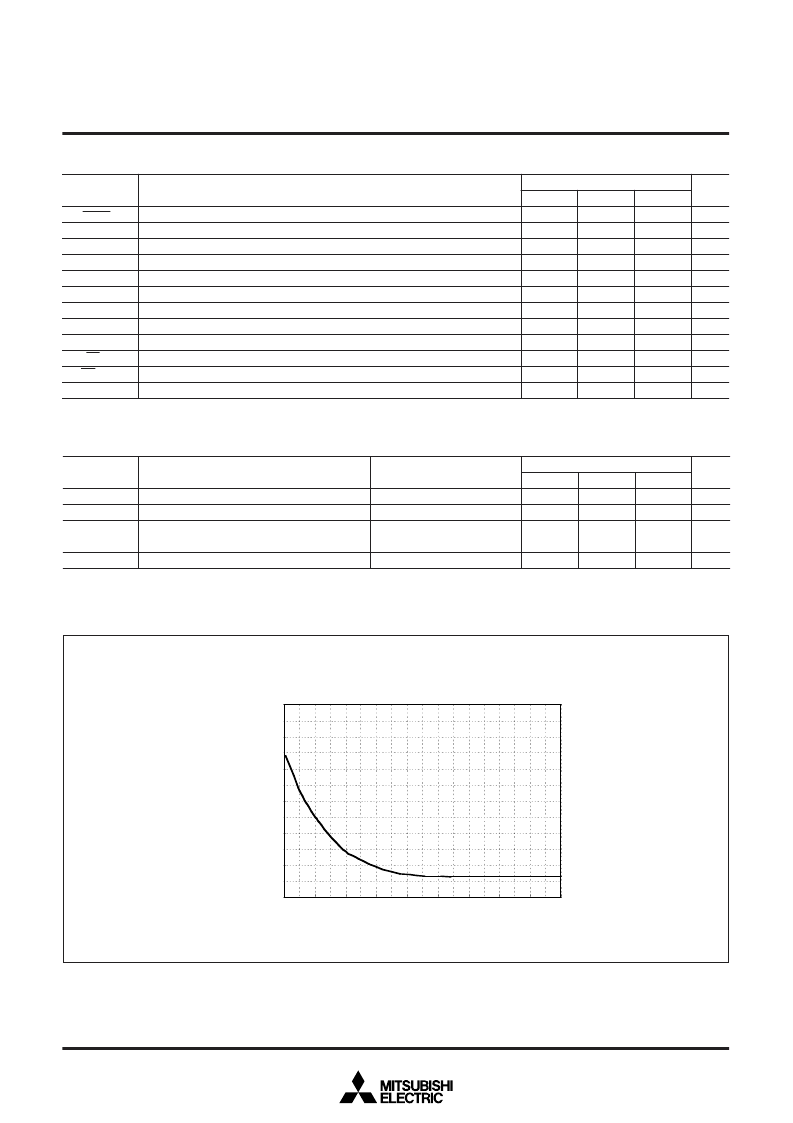
Fig. 13. Standard characteristic example of f(X
IN
)–C
OSC
Reset input “L” pulse width
Main clock input cycle time (X
IN
input)
Main clock input “H” pulse width
Main clock input “L” pulse width
Serial clock input cycle time (Note)
Serial clock input “H” pulse width (Note)
Serial clock input “L” pulse width (Note)
Serial input setup time (Note)
Serial input hold time (Note)
Serial input setup time
Serial input hold time
Serial clock interval time
Limits
Typ.
Min.
2
238
60
60
5
2
3
2
3
50 t
c
(X
IN
)
50 t
c
(X
IN
)
50 t
c
(X
IN
)
Max.
μ
s
ns
ns
ns
CLKs
CLKs
CLKs
CLKs
CLKs
ns
ns
ns
TIMING REQUIREMENTS
(V
CC
= 4.0 to 5.5 V, Ta = –20 to 85 °C, unless otherwise noted)
Parameter
Symbol
Unit
Note
: The unit means a number of noise filter sampling clock (2
tc(X
IN
)).
Serial I/O output delay time (Note 1)
Serial I/O output valid time
High-breakdown-voltage P-channel
open-drain output rising time
External capacitor size (Note 2)
Limits
Typ.
Min.
2
1.8
22
Max.
3
3
CLKs
CLKs
μ
s
pF
SWITCHING CHARACTERISTICS
(V
CC
= 4.0 to 5.5 V, Ta = –20 to 85 °C, unless otherwise noted)
Parameter
Symbol
Unit
C
L
= 100pF
V
EE
= V
CC
–36 V
Test conditions
M
e
a
s
u
r
i
n
g
c
o
n
d
i
t
i
o
n
:
T
a
=
2
5
°
C
,
V
C
C
=
5
.
0
V
2
.
0
1
3
.
0
4
.
0
5
.
0
6
.
0
7
.
0
8
.
0
0
2
0
3
0
4
0
5
0
6
0
7
0
8
0
9
0
1
0
0
F
r
e
q
u
e
n
c
y
f
(
X
I
N
)
[
M
H
z
]
E
x
t
e
r
n
a
l
c
a
p
a
c
i
t
o
r
s
i
z
e C
O
S
C
[
p
F
]
Note 1
: The unit means a number of noise filter sampling clock (2
tc(X
IN
)).
2
: An external capacitor size varies with a mounted condition.
相關(guān)PDF資料 |
PDF描述 |
|---|---|
| M35500 | FLD(VFD) CONTROLLER |
| M35502AFP | FLD CONTROLLER |
| M37100M8 | SINGLE CHIP 8 BIT CMOS MICROCOMPUTER FOR VOLTAGE SYNTHESIZER WITH ON SCREEN DISPLAY CONTROLLER |
| M37100M8-XXXFP | SINGLE CHIP 8 BIT CMOS MICROCOMPUTER FOR VOLTAGE SYNTHESIZER WITH ON SCREEN DISPLAY CONTROLLER |
| M37100M8-XXXSP | SINGLE CHIP 8 BIT CMOS MICROCOMPUTER FOR VOLTAGE SYNTHESIZER WITH ON SCREEN DISPLAY CONTROLLER |
相關(guān)代理商/技術(shù)參數(shù) |
參數(shù)描述 |
|---|---|
| M35501FP | 制造商:MITSUBISHI 制造商全稱:Mitsubishi Electric Semiconductor 功能描述:FLD(VFD) DIGIT EXPANDER |
| M35502AFP | 制造商:MITSUBISHI 制造商全稱:Mitsubishi Electric Semiconductor 功能描述:FLD CONTROLLER |
| M3554 | 制造商:Baldor Electric Company 功能描述: |
| M3558 | 制造商:BALDOR MOTORS 功能描述: 制造商:Baldor Electric Company 功能描述: |
| M3558T | 制造商:BALDOR MOTORS 功能描述: |
發(fā)布緊急采購,3分鐘左右您將得到回復(fù)。