- 您現(xiàn)在的位置:買賣IC網(wǎng) > PDF目錄69011 > M34559G6-XXXFP 4-BIT, MROM, 6 MHz, MICROCONTROLLER, PQFP52 PDF資料下載
參數(shù)資料
| 型號(hào): | M34559G6-XXXFP |
| 元件分類: | 微控制器/微處理器 |
| 英文描述: | 4-BIT, MROM, 6 MHz, MICROCONTROLLER, PQFP52 |
| 封裝: | 10 X 10 MM, 0.65 MM PITCH, PLASTIC, LQFP-52 |
| 文件頁數(shù): | 34/70頁 |
| 文件大小: | 1799K |
| 代理商: | M34559G6-XXXFP |
第1頁第2頁第3頁第4頁第5頁第6頁第7頁第8頁第9頁第10頁第11頁第12頁第13頁第14頁第15頁第16頁第17頁第18頁第19頁第20頁第21頁第22頁第23頁第24頁第25頁第26頁第27頁第28頁第29頁第30頁第31頁第32頁第33頁當(dāng)前第34頁第35頁第36頁第37頁第38頁第39頁第40頁第41頁第42頁第43頁第44頁第45頁第46頁第47頁第48頁第49頁第50頁第51頁第52頁第53頁第54頁第55頁第56頁第57頁第58頁第59頁第60頁第61頁第62頁第63頁第64頁第65頁第66頁第67頁第68頁第69頁第70頁
Rev.1.04
Aug 23, 2007
Page 4 of 146
REJ03B0188-0104
4559 Group
PERFORMANCE OVERVIEW
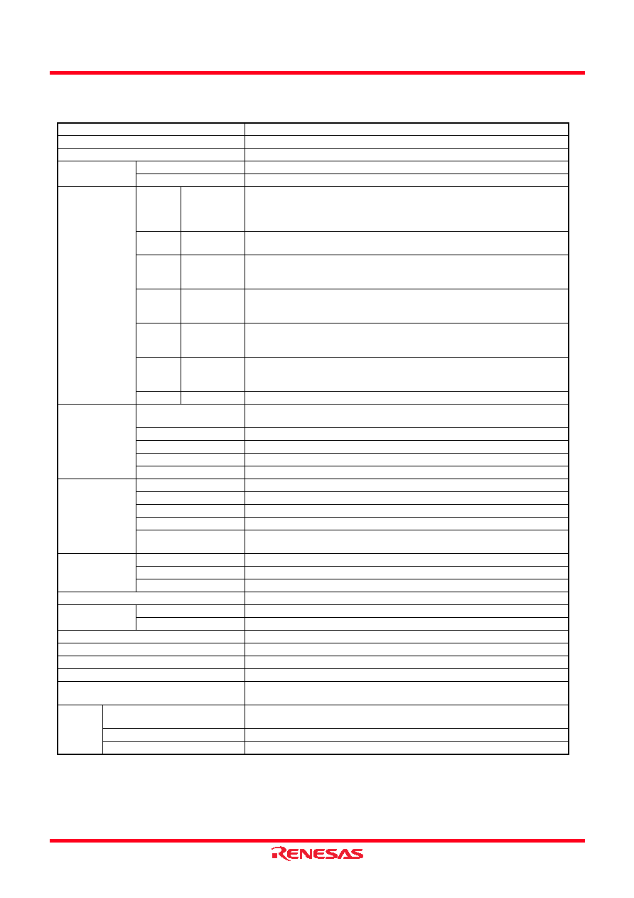
Table 2
Performance overview
Parameter
Function
Number of basic instructions
135
Minimum instruction execution time
0.5
s (Oscillation frequency 6 MHz: high-speed through mode)
Memory sizes
ROM
6144 words
× 10 bits
RAM
288 words
× 4 bits (including LCD display RAM 32 words × 4 bits)
I/O port
D0
D5
I/O
(Input is
examined by
skip decision.)
Six independent I/O ports.
The output structure can be switched by software.
Port D5 is also used as INT pin.
D6, D7
Output
Two independent output ports.
Ports D6 and D7 are also used as XCIN and XCOUT, respectively.
P00
P03
I/O
4-bit I/O port; A pull-up function, a key-on wakeup function and output structure can
be switched by software.
Ports P00
P03 are also used as SEG16SEG19, respectively.
P10
P13
I/O
4-bit I/O port; A pull-up function, a key-on wakeup function and output structure can
be switched by software.
Ports P10
P13 are also used as SEG20SEG23, respectively.
P20
P23
I/O
4-bit I/O port; A pull-up function, a key-on wakeup function and output structure can
be switched by software.
Ports P20
P23 are also used as SEG24SEG27, respectively.
P30
P33
I/O
4-bit I/O port; A pull-up function, a key-on wakeup function and output structure can
be switched by software.
Ports P30
P33 are also used as SEG28SEG31, respectively.
C
Output
1-bit output; Port C is also used as CNTR pin.
Timer
Timer 1
8-bit timer with a reload register and carrier wave output auto-control function,
and has an event counter.
Timer 2
8-bit timer with two reload registers and carrier wave generation function.
Timer 3
16-bit timer, fixed dividing frequency (timer for clock count)
Timer LC
4-bit programmable timer with a reload register (for LCD clock generating)
Watchdog timer
16-bit timer, fixed dividing frequency (timer for monitor)
LCD control circuit
Selective bias value
1/2, 1/3 bias
Selective duty value
2, 3, 4 duty
Common output
4
Segment output
32
Internal resistor for power
supply
2r
× 3, 2r × 2, r × 3, r × 2 (r = 100 k, (Ta = 25 °C, Typical value))
Voltage drop
detection circuit
Reset occurrence
Typ. 1.7 V (Ta=25 °C)
Reset release
Typ. 1.8 V (Ta=25 °C)
Skip occurrence
Typ. 2.0 V (Ta=25 °C)
Power-on reset circuit
Built-in
Interrupt
Source
4 sources (one for external, three for timers)
Nesting
1 level
Subroutine nesting
8 levels
Device structure
CMOS silicon gate
Package
52-pin plastic molded LQFP (PLQP0052JA-A)
Operating temperature range
-20 to 85 °C
Power source voltage
1.8 to 5.5 V (It depends on operation source clock, oscillation frequency and
operation mode)
Power
dissipation
(Typ. value)
At active mode
0.3 mA (Ta = 25 °C, VDD
= 3 V, f(XIN) = 4 MHz, f(XCIN) = stop, f(RING) = stop,
f(STCK) = f(XIN)/8
At clock operating mode
5
A (Ta = 25 °C, VDD = 3 V, f(XCIN) = 32 kHz)
At RAM back-up
0.1
A (Ta = 25 °C, VDD = 5 V, output transistor is cut-off state)
相關(guān)PDF資料 |
PDF描述 |
|---|---|
| M34570EDFP | 4-BIT, OTPROM, 2 MHz, MICROCONTROLLER, PDSO36 |
| M34570M4-XXXFP | 4-BIT, MROM, 2 MHz, MICROCONTROLLER, PDSO36 |
| M34570M8-XXXFP | 4-BIT, MROM, MICROCONTROLLER, PDSO36 |
| M34570EDFP | 4-BIT, OTPROM, MICROCONTROLLER, PDSO36 |
| M34584EDFP | 4-BIT, OTPROM, 6 MHz, MICROCONTROLLER, PDSO42 |
相關(guān)代理商/技術(shù)參數(shù) |
參數(shù)描述 |
|---|---|
| M3455AG8FP | 制造商:RENESAS 制造商全稱:Renesas Technology Corp 功能描述:SINGLE-CHIP 4-BIT CMOS MICROCOMPUTER |
| M3455AG8-XXXFP | 制造商:RENESAS 制造商全稱:Renesas Technology Corp 功能描述:SINGLE-CHIP 4-BIT CMOS MICROCOMPUTER |
| M3455AGCFP | 制造商:RENESAS 制造商全稱:Renesas Technology Corp 功能描述:SINGLE-CHIP 4-BIT CMOS MICROCOMPUTER |
| M3455AGC-XXXFP | 制造商:RENESAS 制造商全稱:Renesas Technology Corp 功能描述:SINGLE-CHIP 4-BIT CMOS MICROCOMPUTER |
| M3455-SL001 | 制造商:Alpha Wire 功能描述: |
發(fā)布緊急采購,3分鐘左右您將得到回復(fù)。