- 您現(xiàn)在的位置:買賣IC網(wǎng) > PDF目錄45027 > M34553M4-XXXFP 4-BIT, MROM, 6 MHz, MICROCONTROLLER, PQFP48 PDF資料下載
參數(shù)資料
| 型號(hào): | M34553M4-XXXFP |
| 元件分類: | 微控制器/微處理器 |
| 英文描述: | 4-BIT, MROM, 6 MHz, MICROCONTROLLER, PQFP48 |
| 封裝: | 7 X 7 MM, 0.50 MM PITCH, PLASTIC, LQFP-48 |
| 文件頁(yè)數(shù): | 99/147頁(yè) |
| 文件大小: | 1098K |
| 代理商: | M34553M4-XXXFP |
第1頁(yè)第2頁(yè)第3頁(yè)第4頁(yè)第5頁(yè)第6頁(yè)第7頁(yè)第8頁(yè)第9頁(yè)第10頁(yè)第11頁(yè)第12頁(yè)第13頁(yè)第14頁(yè)第15頁(yè)第16頁(yè)第17頁(yè)第18頁(yè)第19頁(yè)第20頁(yè)第21頁(yè)第22頁(yè)第23頁(yè)第24頁(yè)第25頁(yè)第26頁(yè)第27頁(yè)第28頁(yè)第29頁(yè)第30頁(yè)第31頁(yè)第32頁(yè)第33頁(yè)第34頁(yè)第35頁(yè)第36頁(yè)第37頁(yè)第38頁(yè)第39頁(yè)第40頁(yè)第41頁(yè)第42頁(yè)第43頁(yè)第44頁(yè)第45頁(yè)第46頁(yè)第47頁(yè)第48頁(yè)第49頁(yè)第50頁(yè)第51頁(yè)第52頁(yè)第53頁(yè)第54頁(yè)第55頁(yè)第56頁(yè)第57頁(yè)第58頁(yè)第59頁(yè)第60頁(yè)第61頁(yè)第62頁(yè)第63頁(yè)第64頁(yè)第65頁(yè)第66頁(yè)第67頁(yè)第68頁(yè)第69頁(yè)第70頁(yè)第71頁(yè)第72頁(yè)第73頁(yè)第74頁(yè)第75頁(yè)第76頁(yè)第77頁(yè)第78頁(yè)第79頁(yè)第80頁(yè)第81頁(yè)第82頁(yè)第83頁(yè)第84頁(yè)第85頁(yè)第86頁(yè)第87頁(yè)第88頁(yè)第89頁(yè)第90頁(yè)第91頁(yè)第92頁(yè)第93頁(yè)第94頁(yè)第95頁(yè)第96頁(yè)第97頁(yè)第98頁(yè)當(dāng)前第99頁(yè)第100頁(yè)第101頁(yè)第102頁(yè)第103頁(yè)第104頁(yè)第105頁(yè)第106頁(yè)第107頁(yè)第108頁(yè)第109頁(yè)第110頁(yè)第111頁(yè)第112頁(yè)第113頁(yè)第114頁(yè)第115頁(yè)第116頁(yè)第117頁(yè)第118頁(yè)第119頁(yè)第120頁(yè)第121頁(yè)第122頁(yè)第123頁(yè)第124頁(yè)第125頁(yè)第126頁(yè)第127頁(yè)第128頁(yè)第129頁(yè)第130頁(yè)第131頁(yè)第132頁(yè)第133頁(yè)第134頁(yè)第135頁(yè)第136頁(yè)第137頁(yè)第138頁(yè)第139頁(yè)第140頁(yè)第141頁(yè)第142頁(yè)第143頁(yè)第144頁(yè)第145頁(yè)第146頁(yè)第147頁(yè)
Rev.3.02
Dec 22, 2006
page 53 of 142
REJ03B0024-0302
4553 Group
(6) Return signal
An external wakeup signal or timer 3 interrupt request flag (T3F) is
used to return from the clock operating mode.
An external wakeup signal is used to return from the RAM back-up
mode because the oscillation is stopped.
Table 16 shows the return condition for each return source.
(7) Control registers
Key-on wakeup control register K0
Register K0 controls the ports P0 and P1 key-on wakeup func-
tion. Set the contents of this register through register A with the
TK0A instruction. In addition, the TAK0 instruction can be used to
transfer the contents of register K0 to register A.
Key-on wakeup control register K1
Register K1 controls the return condition and the selection of
valid waveform/level of port P1. Set the contents of this register
through register A with the TK1A instruction. In addition, the TAK1
instruction can be used to transfer the contents of register K0 to
register A.
Key-on wakeup control register K2
Register K2 controls the INT pin key-on wakeup function and the
selection of return codition. Set the contents of this register
through register A with the TK2A instruction. In addition, the TAK2
instruction can be used to transfer the contents of register K2 to
register A.
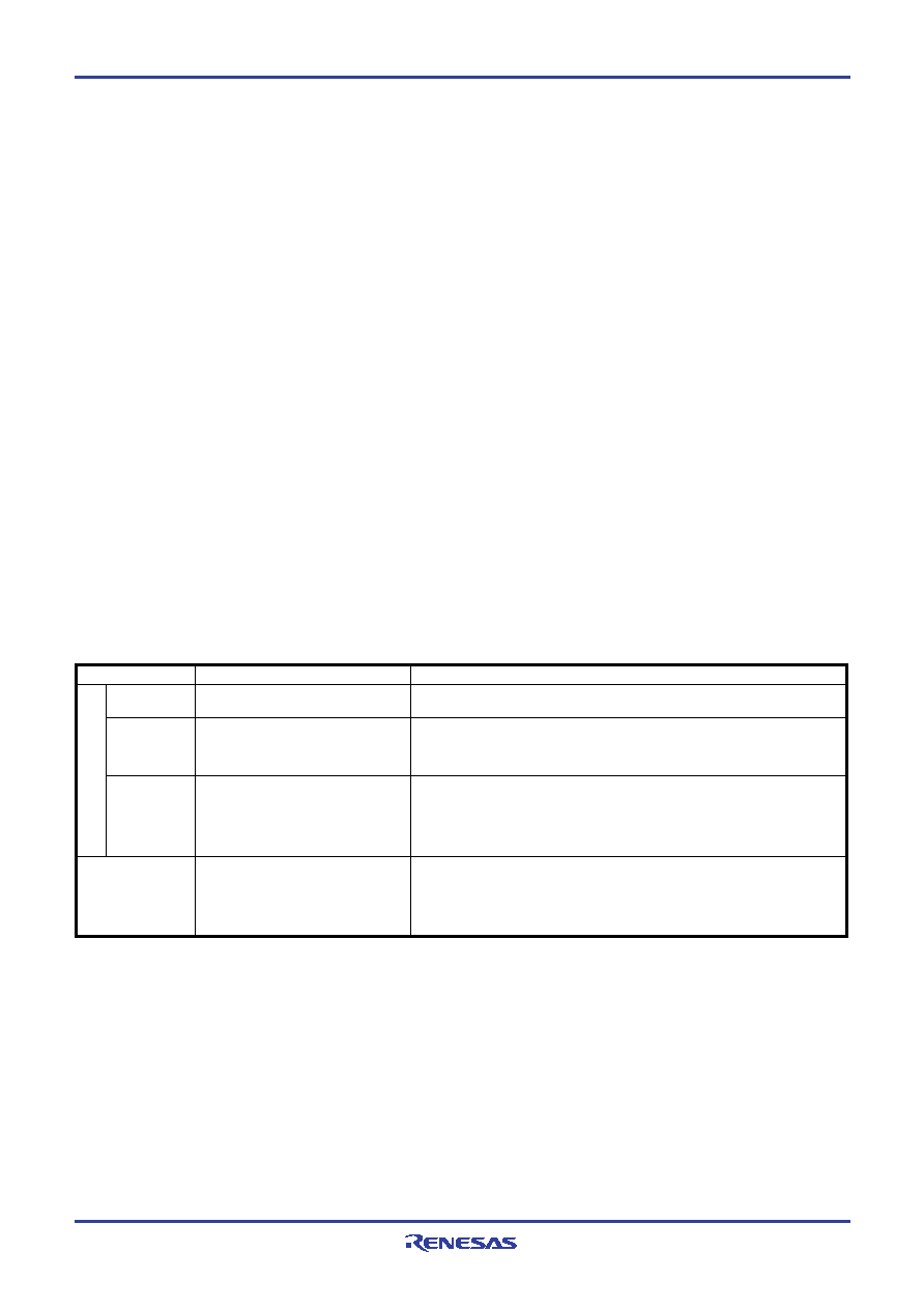
Table 16 Return source and return condition
Remarks
Return condition
External
wakeup
signal
Return source
Ports P00–P03
Ports P10–P13
INT pin
Pull-up control register PU0
Register PU0 controls the ON/OFF of the port P0 pull-up transis-
tor. Set the contents of this register through register A with the
TPU0A instruction. In addition, the TAPU0 instruction can be
used to transfer the contents of register PU0 to register A.
Pull-up control register PU1
Register PU1 controls the ON/OFF of the port P1 pull-up transis-
tor. Set the contents of this register through register A with the
TPU1A instruction. In addition, the TAPU1 instruction can be
used to transfer the contents of register PU1 to register A.
External interrupt control register I1
Register I1 controls the valid waveform of the external 0 inter-
rupt, the input control of INT pin and the return input level. Set
the contents of this register through register A with the TI1A in-
struction. In addition, the TAI1 instruction can be used to transfer
the contents of register I1 to register A.
Return by an external falling edge
(“H”
→“L”).
Return by an external “H” level or “L”
level input, or rising edge (“L”
→“H”)
or falling edge (“H”
→“L”).
Return by an external “L” level input.
Return by an external “H” level or “L”
level input, or rising edge (“L”
→“H”)
or falling edge (“H”
→“L”).
When the return level is input, the in-
terrupt request flag (EXF0) is not set.
Return by timer 3 underflow or by
setting T3F to “1”.
It can be used in the clock operating
mode.
The key-on wakeup function can be selected by two port unit.
The key-on wakeup function can be selected by two port unit. Select the re-
turn level (“L” level or “H” level) and return condition (return by level or
edge) with register K1 according to the external state before going into the
power down state.
Select the return level (“L” level or “H” level) with register I1 and return con-
dition (return by level or edge) with register K2 according to the external
state before going into the power down state.
Clear T3F with the SNZT3 instruction before system enters into the power
down state.
When system enters into the power down state while T3F is “1”, system re-
turns from the state immediately because it is recognized as return
condition.
Timer 3 interrupt
request flag (T3F)
相關(guān)PDF資料 |
PDF描述 |
|---|---|
| M34553M8H-XXXFP | 4-BIT, MROM, 6 MHz, MICROCONTROLLER, PQFP48 |
| M34554MC-XXXFP | 4-BIT, MROM, 6 MHz, MICROCONTROLLER, PQFP64 |
| M34554EDFP | 4-BIT, OTPROM, 6 MHz, MICROCONTROLLER, PQFP64 |
| M3455AG8-XXXFP | 4-BIT, OTPROM, 6 MHz, MICROCONTROLLER, PQFP52 |
| M3455AGCFP | 4-BIT, OTPROM, 6 MHz, MICROCONTROLLER, PQFP52 |
相關(guān)代理商/技術(shù)參數(shù) |
參數(shù)描述 |
|---|---|
| M34553M8H-XXXFP | 制造商:RENESAS 制造商全稱:Renesas Technology Corp 功能描述:SINGLE-CHIP 4-BIT CMOS MICROCOMPUTER |
| M34553M8-XXXFP | 制造商:RENESAS 制造商全稱:Renesas Technology Corp 功能描述:SINGLE-CHIP 4-BIT CMOS MICROCOMPUTER |
| M34553MXH-XXXFP | 制造商:RENESAS 制造商全稱:Renesas Technology Corp 功能描述:SINGLE-CHIP 4-BIT CMOS MICROCOMPUTER |
| M34553MX-XXXFP | 制造商:RENESAS 制造商全稱:Renesas Technology Corp 功能描述:SINGLE-CHIP 4-BIT CMOS MICROCOMPUTER |
| M34553T-PTCA | 制造商:RENESAS 制造商全稱:Renesas Technology Corp 功能描述:50-pin Narrow-Pitch Connector Converter Board for M34552T2-CPE(for 4553, 4556 Group) |
發(fā)布緊急采購(gòu),3分鐘左右您將得到回復(fù)。