- 您現(xiàn)在的位置:買賣IC網(wǎng) > PDF目錄67761 > M34518M2-XXXFP 4-BIT, MROM, 6 MHz, MICROCONTROLLER, PQFP32 PDF資料下載
參數(shù)資料
| 型號(hào): | M34518M2-XXXFP |
| 元件分類: | 微控制器/微處理器 |
| 英文描述: | 4-BIT, MROM, 6 MHz, MICROCONTROLLER, PQFP32 |
| 封裝: | 7 X 7 MM, 0.80 MM PITCH, PLASTIC, LQFP-32 |
| 文件頁(yè)數(shù): | 122/162頁(yè) |
| 文件大小: | 1149K |
| 代理商: | M34518M2-XXXFP |
第1頁(yè)第2頁(yè)第3頁(yè)第4頁(yè)第5頁(yè)第6頁(yè)第7頁(yè)第8頁(yè)第9頁(yè)第10頁(yè)第11頁(yè)第12頁(yè)第13頁(yè)第14頁(yè)第15頁(yè)第16頁(yè)第17頁(yè)第18頁(yè)第19頁(yè)第20頁(yè)第21頁(yè)第22頁(yè)第23頁(yè)第24頁(yè)第25頁(yè)第26頁(yè)第27頁(yè)第28頁(yè)第29頁(yè)第30頁(yè)第31頁(yè)第32頁(yè)第33頁(yè)第34頁(yè)第35頁(yè)第36頁(yè)第37頁(yè)第38頁(yè)第39頁(yè)第40頁(yè)第41頁(yè)第42頁(yè)第43頁(yè)第44頁(yè)第45頁(yè)第46頁(yè)第47頁(yè)第48頁(yè)第49頁(yè)第50頁(yè)第51頁(yè)第52頁(yè)第53頁(yè)第54頁(yè)第55頁(yè)第56頁(yè)第57頁(yè)第58頁(yè)第59頁(yè)第60頁(yè)第61頁(yè)第62頁(yè)第63頁(yè)第64頁(yè)第65頁(yè)第66頁(yè)第67頁(yè)第68頁(yè)第69頁(yè)第70頁(yè)第71頁(yè)第72頁(yè)第73頁(yè)第74頁(yè)第75頁(yè)第76頁(yè)第77頁(yè)第78頁(yè)第79頁(yè)第80頁(yè)第81頁(yè)第82頁(yè)第83頁(yè)第84頁(yè)第85頁(yè)第86頁(yè)第87頁(yè)第88頁(yè)第89頁(yè)第90頁(yè)第91頁(yè)第92頁(yè)第93頁(yè)第94頁(yè)第95頁(yè)第96頁(yè)第97頁(yè)第98頁(yè)第99頁(yè)第100頁(yè)第101頁(yè)第102頁(yè)第103頁(yè)第104頁(yè)第105頁(yè)第106頁(yè)第107頁(yè)第108頁(yè)第109頁(yè)第110頁(yè)第111頁(yè)第112頁(yè)第113頁(yè)第114頁(yè)第115頁(yè)第116頁(yè)第117頁(yè)第118頁(yè)第119頁(yè)第120頁(yè)第121頁(yè)當(dāng)前第122頁(yè)第123頁(yè)第124頁(yè)第125頁(yè)第126頁(yè)第127頁(yè)第128頁(yè)第129頁(yè)第130頁(yè)第131頁(yè)第132頁(yè)第133頁(yè)第134頁(yè)第135頁(yè)第136頁(yè)第137頁(yè)第138頁(yè)第139頁(yè)第140頁(yè)第141頁(yè)第142頁(yè)第143頁(yè)第144頁(yè)第145頁(yè)第146頁(yè)第147頁(yè)第148頁(yè)第149頁(yè)第150頁(yè)第151頁(yè)第152頁(yè)第153頁(yè)第154頁(yè)第155頁(yè)第156頁(yè)第157頁(yè)第158頁(yè)第159頁(yè)第160頁(yè)第161頁(yè)第162頁(yè)
Rev.3.01
2005.06.15
page 60 of 157
REJ03B0008-0301
4518 Group
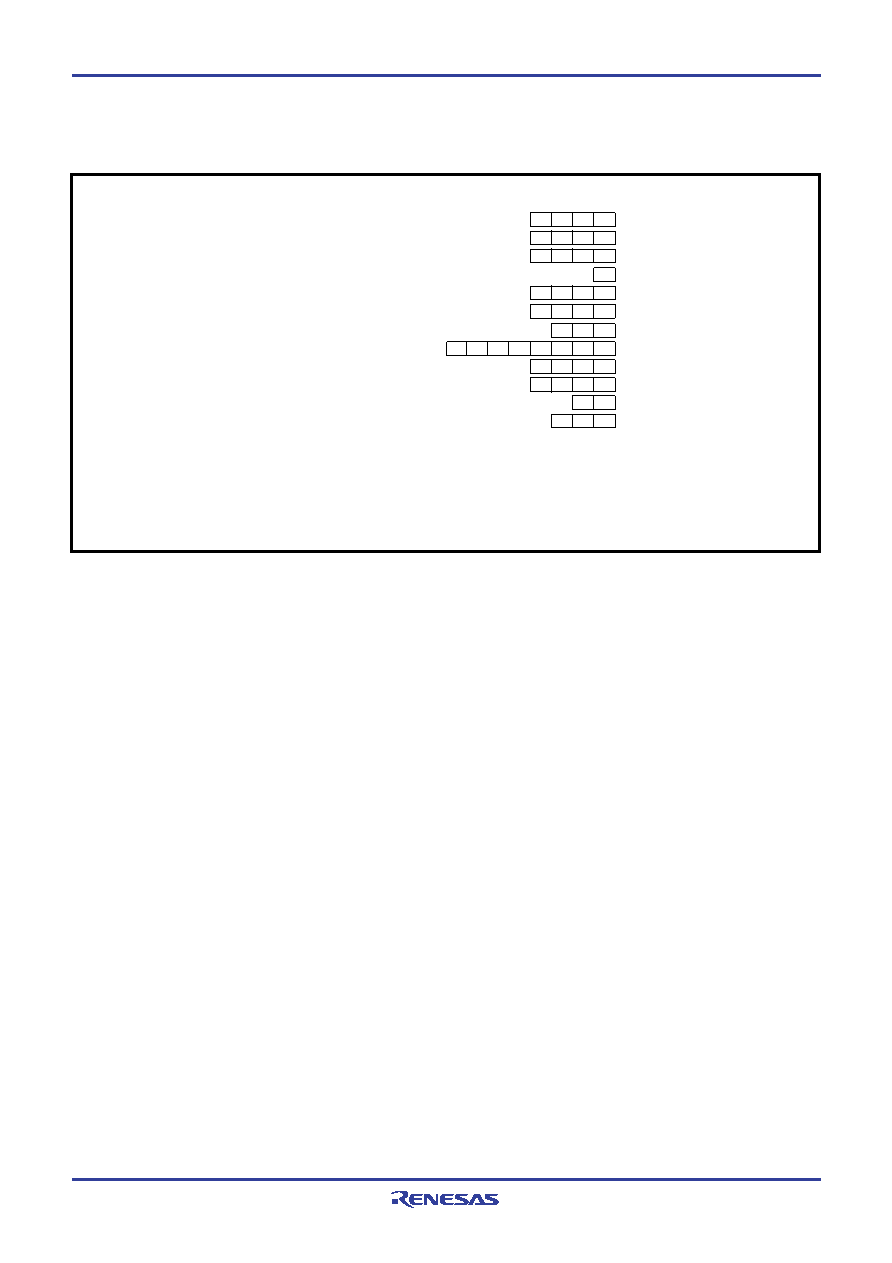
Port output structure control register FR0 ...........................................................................
Port output structure control register FR1 ...........................................................................
Port output structure control register FR2 ...........................................................................
Carry flag (CY) ......................................................................................................................
Register A .............................................................................................................................
Register B .............................................................................................................................
Register D .............................................................................................................................
Register E .............................................................................................................................
Register X .............................................................................................................................
Register Y .............................................................................................................................
Register Z .............................................................................................................................
Stack pointer (SP) ................................................................................................................
Operation source clock .......................................................... On-chip oscillator (operating)
Ceramic resonator circuit .............................................................................................. Stop
RC oscillation circuit ...................................................................................................... Stop
Quartz-crystal oscillation circuit .................................................................................... Stop
“” represents undefined.
Fig. 50 Internal state at reset 2
00
0
00
00
11
1
相關(guān)PDF資料 |
PDF描述 |
|---|---|
| M34519M6-XXXFP | 4-BIT, MROM, 6 MHz, MICROCONTROLLER, PDSO42 |
| M34519M8-XXXFP | 4-BIT, MROM, 6 MHz, MICROCONTROLLER, PDSO42 |
| M34519E8FP | 4-BIT, OTPROM, 6 MHz, MICROCONTROLLER, PDSO42 |
| M34519M8-XXXFP | 4-BIT, MROM, 6 MHz, MICROCONTROLLER, PDSO42 |
| M34519M6-XXXFP | 4-BIT, MROM, 6 MHz, MICROCONTROLLER, PDSO42 |
相關(guān)代理商/技術(shù)參數(shù) |
參數(shù)描述 |
|---|---|
| M34518M2-XXXSP | 制造商:RENESAS 制造商全稱:Renesas Technology Corp 功能描述:SINGLE-CHIP 4-BIT CMOS MICROCOMPUTER |
| M34518M4-XXXFP | 制造商:RENESAS 制造商全稱:Renesas Technology Corp 功能描述:SINGLE-CHIP 4-BIT CMOS MICROCOMPUTER |
| M34518M4-XXXSP | 制造商:RENESAS 制造商全稱:Renesas Technology Corp 功能描述:SINGLE-CHIP 4-BIT CMOS MICROCOMPUTER |
| M34518M6-XXXFP | 制造商:RENESAS 制造商全稱:Renesas Technology Corp 功能描述:SINGLE-CHIP 4-BIT CMOS MICROCOMPUTER |
| M34518M8-XXXFP | 制造商:RENESAS 制造商全稱:Renesas Technology Corp 功能描述:SINGLE-CHIP 4-BIT CMOS MICROCOMPUTER |
發(fā)布緊急采購(gòu),3分鐘左右您將得到回復(fù)。