- 您現(xiàn)在的位置:買賣IC網(wǎng) > PDF目錄69010 > M34250M2-XXXFP 4-BIT, MROM, 4.4 MHz, MICROCONTROLLER, PDSO20 PDF資料下載
參數(shù)資料
| 型號: | M34250M2-XXXFP |
| 元件分類: | 微控制器/微處理器 |
| 英文描述: | 4-BIT, MROM, 4.4 MHz, MICROCONTROLLER, PDSO20 |
| 封裝: | PLASTIC, SOP-20 |
| 文件頁數(shù): | 45/59頁 |
| 文件大小: | 713K |
| 代理商: | M34250M2-XXXFP |
第1頁第2頁第3頁第4頁第5頁第6頁第7頁第8頁第9頁第10頁第11頁第12頁第13頁第14頁第15頁第16頁第17頁第18頁第19頁第20頁第21頁第22頁第23頁第24頁第25頁第26頁第27頁第28頁第29頁第30頁第31頁第32頁第33頁第34頁第35頁第36頁第37頁第38頁第39頁第40頁第41頁第42頁第43頁第44頁當(dāng)前第45頁第46頁第47頁第48頁第49頁第50頁第51頁第52頁第53頁第54頁第55頁第56頁第57頁第58頁第59頁
4
MITSUBISHI MICROCOMPUTERS
4250 Group
SINGLE-CHIP 4-BIT CMOS MICROCOMPUTER
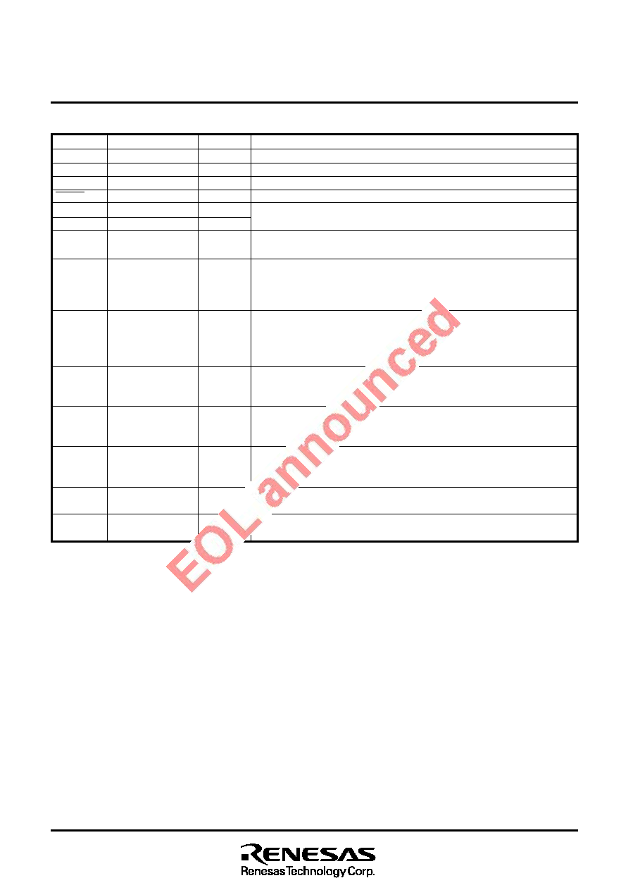
PIN DESCRIPTION
Name
Power supply
Ground
CNVSS
Reset input
System clock input
System clock output
I/O port F
I/O port G
I/O port S
I/O port D
I/O port C
I/O port K
Timer output
Interrupt input
Input/Output
—
Input
Output
I/O
Output
Input
Function
Connected to a plus power supply.
Connected to a 0 V power supply.
Connect CNVSS to VSS and apply “L” (0V) to CNVSS certainly.
Reset pulse input pin
I/O pins of the system clock generating circuit. Connect pins XIN and XOUT directly.
Then, pull up XIN pin through a resistor and pull down XOUT pin through a capacitor.
2-bit I/O port; for input use, set the latch of the specified bit to “1.” The output
structure is N-channel open-drain.
4-bit I/O port. For input use, set the latch of the specified bit to “1.” The output
structure is N-channel open-drain. Every pin of the ports has a key-on wakeup
function and a pull-up function. Both functions can be switched by software.
Ports G0 and G1 are also used as pins INT and TOUT, respectively.
4-bit I/O port. For input use, set the latch of the specified bit to “1.” The output
structure is N-channel open-drain. Every pin of the ports has a key-on wakeup
function which can be switched by software. Also, it is used to perform the logic
operation using register A.
Each pin of port D has an independent 1-bit wide I/O function. For input use, set
the latch of the specified bit to “1.” The output structure is N-channel open-drain.
Ports D2 and D3 are also used as ports C and K, respectively.
1-bit I/O port. For input use, set the latch of the specified bit to “1.” The output
structure is N-channel open-drain. Port C has a pull-up function which can be
switched by software. It is also used as port D2.
1-bit I/O port. For input use, set the latch of the specified bit to “1.” The output
structure is N-channel open-drain. Port K has a pull-up function which can be
switched by software. It is also used as port D3.
TOUT pin has the function to output the timer 1 underflow signal divided by 2. It is
also used as port G1.
INT pin accepts an external interrupt. It also accepts the input signal to return the
system from the RAM back-up state. It is also used as port G0.
Pin
VDD
VSS
CNVSS
RESET
XIN
XOUT
F0, F1
G0–G3
S0–S3
D0–D3
C
K
TOUT
INT
相關(guān)PDF資料 |
PDF描述 |
|---|---|
| M34280M1-XXXFP | 4-BIT, MROM, 4 MHz, MICROCONTROLLER, PDSO20 |
| M34280M1-XXXGP | 4-BIT, MROM, 4 MHz, MICROCONTROLLER, PDSO20 |
| M34280E1GP | 4-BIT, OTPROM, 4 MHz, MICROCONTROLLER, PDSO20 |
| M34501M2-XXXFP | 4-BIT, MROM, 4.4 MHz, MICROCONTROLLER, PDSO20 |
| M34501E4FP | 4-BIT, OTPROM, 4.4 MHz, MICROCONTROLLER, PDSO20 |
相關(guān)代理商/技術(shù)參數(shù) |
參數(shù)描述 |
|---|---|
| M3426 SL002 | 制造商:Alpha Wire 功能描述:CBL 8PR 24AWG SLT 500' |
| M3426 SL005 | 制造商:Alpha Wire 功能描述:CBL 8PR 24AWG SLT 100' |
| M3427-SLATE-500 | 制造商:Alpha Wire 功能描述: |
| M3428 SL001 | 制造商:Alpha Wire 功能描述:CBL 12PR 24AWG SLT 1000' |
| M3428 SL002 | 制造商:Alpha Wire 功能描述:CBL 12PR 24AWG SLT 500' |
發(fā)布緊急采購,3分鐘左右您將得到回復(fù)。