- 您現(xiàn)在的位置:買賣IC網(wǎng) > PDF目錄69009 > M306H7MG-XXXFP 16-BIT, MROM, 16 MHz, MICROCONTROLLER, PQFP100 PDF資料下載
參數(shù)資料
| 型號: | M306H7MG-XXXFP |
| 元件分類: | 微控制器/微處理器 |
| 英文描述: | 16-BIT, MROM, 16 MHz, MICROCONTROLLER, PQFP100 |
| 封裝: | 14 X 20 MM, 0.65 MM PITCH, PLASTIC, QFP-100 |
| 文件頁數(shù): | 177/180頁 |
| 文件大小: | 2820K |
| 代理商: | M306H7MG-XXXFP |
第1頁第2頁第3頁第4頁第5頁第6頁第7頁第8頁第9頁第10頁第11頁第12頁第13頁第14頁第15頁第16頁第17頁第18頁第19頁第20頁第21頁第22頁第23頁第24頁第25頁第26頁第27頁第28頁第29頁第30頁第31頁第32頁第33頁第34頁第35頁第36頁第37頁第38頁第39頁第40頁第41頁第42頁第43頁第44頁第45頁第46頁第47頁第48頁第49頁第50頁第51頁第52頁第53頁第54頁第55頁第56頁第57頁第58頁第59頁第60頁第61頁第62頁第63頁第64頁第65頁第66頁第67頁第68頁第69頁第70頁第71頁第72頁第73頁第74頁第75頁第76頁第77頁第78頁第79頁第80頁第81頁第82頁第83頁第84頁第85頁第86頁第87頁第88頁第89頁第90頁第91頁第92頁第93頁第94頁第95頁第96頁第97頁第98頁第99頁第100頁第101頁第102頁第103頁第104頁第105頁第106頁第107頁第108頁第109頁第110頁第111頁第112頁第113頁第114頁第115頁第116頁第117頁第118頁第119頁第120頁第121頁第122頁第123頁第124頁第125頁第126頁第127頁第128頁第129頁第130頁第131頁第132頁第133頁第134頁第135頁第136頁第137頁第138頁第139頁第140頁第141頁第142頁第143頁第144頁第145頁第146頁第147頁第148頁第149頁第150頁第151頁第152頁第153頁第154頁第155頁第156頁第157頁第158頁第159頁第160頁第161頁第162頁第163頁第164頁第165頁第166頁第167頁第168頁第169頁第170頁第171頁第172頁第173頁第174頁第175頁第176頁當(dāng)前第177頁第178頁第179頁第180頁
Rev.2.10
Oct 25, 2006
Page 94 of 326
REJ03B0152-0210
M306H7MG-XXXFP/MC-XXXFP/FGFP
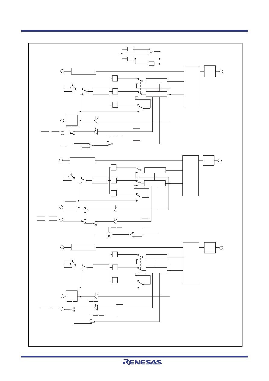
10. SERIAL I/O
Figure 10.1
UARTi Block Diagram
Clock synchronous type
(when internal clock is selected)
Clock synchronous type
(when external clock is selected)
Clock source selection
Internal
External
CTS/RTS disabled
CTS/RTS selected
RxD0
1 / (n0+1)
1/16
1/2
U0BRG
register
CLK0
CTS0 / RTS0
f1SIO or f2SIO
f8SIO
f32SIO
RTS0
CTS0
TxD0
(UART0)
f1SIO or f2SIO
1/2
1/8
f8SIO
1/4
f32SIO
f1SIO
f2SIO
PCLK1=0
PCLK1=1
CLK1 to CLK0
002
012
102
CKDIR=0
CKDIR=1
CKPOL
CKDIR=0
CKDIR=1
CRS=1
CRS=0
CRD=0
CRD=1
RCSP=0
RCSP=1
“H”
CRD=0
CRD=1
RxD polarity
reversing circuit
Main clock
UART reception
Clock synchronous
type
UART transmission
Clock synchronous
type
Clock synchronous type
(when internal clock is selected)
Receive
clock
Transmit
clock
Reception
control circuit
Transmission control
circuit
Transmit/
receive
unit
TxD
polarity
reversing
circuit
CLK
polarity
reversing
circuit
CTS/RTS disabled
CTS0 from UART1
UART reception
Clock synchronous
type
RxD1
TxD1
(UART1)
1 / (n1+1)
1/16
1/2
U1BRG
register
CLK1
f1SIO or f2SIO
f8SIO
f32SIO
CLK1 to CLK0
002
012
102
CKDIR=0
CKDIR=1
CKPOL
CKDIR=0
CKDIR=1
CRD=0
CRD=1
CLKMD0=0
CLKMD1=0
CRS=1
CRS=0
RCSP=0
RCSP=1
CLKMD0=1
CLKMD1=1
RxD polarity
reversing circuit
Clock source selection
Internal
External
UART transmission
Clock synchronous
type
Clock synchronous type
(when internal clock is selected)
Receive
clock
Transmit
clock
Reception
control circuit
Transmission
control circuit
Transmit/
receive
unit
TxD
polarity
reversing
circuit
Clock synchronous type
(when external clock is selected)
Clock synchronous type
(when internal clock is selected)
CLK
polarity
reversing
circuit
RTS1
CTS1
Clock output
pin select
CTS/RTS disabled
CTS/RTS selected
CTS0 from UART0
CTS1 / RTS1/
CTS0/ CLKS1
Note: UART2 is the N-channel open-drain output. Cannot be set to the CMOS output.
i = 0 to 2
ni: Values set to the UiBRG register
SMD2 to SMD0, CKDIR: UiMR register's bits
CLK1 to CLK0, CKPOL, CRD, CRS: UiC0 register's bits
CLKMD0, CLKMD1, RCSP: UCON register's bits
RxD2
CLK2
CTS2 / RTS2
RTS2
CTS2
TxD2
(UART2)
1 / (n2+1)
1/16
1/2
U2BRG
register
f1SIO or f2SIO
f8SIO
f32SIO
CLK1 to CLK0
002
012
102
CKDIR=0
CKDIR=1
CKPOL
CKDIR=0
CKDIR=1
CRS=1
CRS=0
CRD=0
CRD=1
Reception
control circuit
Transmission
control circuit
UART reception
Clock synchronous
type
UART transmission
Clock synchronous
type
Clock synchronous type
(when internal clock is selected)
Receive
clock
Transmit
clock
RxD polarity
reversing circuit
Internal
External
Clock source selection
TxD
polarity
reversing
circuit
Transmit/
receive
unit
(Note)
Clock synchronous type
(when internal clock is selected)
Clock synchronous type
(when external clock is selected)
CLK
polarity
reversing
circuit
CTS/RTS disabled
CTS/RTS
selected
相關(guān)PDF資料 |
PDF描述 |
|---|---|
| M306H7FGFP | 16-BIT, FLASH, 16 MHz, MICROCONTROLLER, PQFP100 |
| M306K7F8LRP | 16-BIT, FLASH, 8 MHz, MICROCONTROLLER, PQFP144 |
| M306K9FCLRP | 16-BIT, FLASH, 16 MHz, MICROCONTROLLER, PQFP144 |
| M306K9F8LRP | 16-BIT, FLASH, 16 MHz, MICROCONTROLLER, PQFP144 |
| M306KAFCLRP | 16-BIT, FLASH, 16 MHz, MICROCONTROLLER, PQFP144 |
相關(guān)代理商/技術(shù)參數(shù) |
參數(shù)描述 |
|---|---|
| M306K7F8LRP | 制造商:RENESAS 制造商全稱:Renesas Technology Corp 功能描述:SINGLE-CHIP 16-BIT CMOS MICROCOMPUTER |
| M306K9FCLRP | 制造商:RENESAS 制造商全稱:Renesas Technology Corp 功能描述:SINGLE-CHIP 16-BIT CMOS MICROCOMPUTER |
| M306K9T2-CPE | 功能描述:M-SUPPORT TOOL RoHS:否 類別:編程器,開發(fā)系統(tǒng) >> 內(nèi)電路編程器、仿真器以及調(diào)試器 系列:- 產(chǎn)品變化通告:Development Systems Discontinuation 19/Jul/2010 標(biāo)準(zhǔn)包裝:1 系列:* 類型:* 適用于相關(guān)產(chǎn)品:* 所含物品:* |
| M306KAFCLRP | 制造商:RENESAS 制造商全稱:Renesas Technology Corp 功能描述:SINGLE-CHIP 16-BIT CMOS MICROCOMPUTER Description |
| M306N0FG | 制造商:MITSUBISHI 制造商全稱:Mitsubishi Electric Semiconductor 功能描述:SINGLE-CHIP 16-BIT CMOS MICROCOMPUTER |
發(fā)布緊急采購,3分鐘左右您將得到回復(fù)。