- 您現(xiàn)在的位置:買賣IC網(wǎng) > PDF目錄359009 > M28C64X-150K6 (意法半導(dǎo)體) 64 Kbit 8Kb x8 Parallel EEPROM PDF資料下載
參數(shù)資料
| 型號(hào): | M28C64X-150K6 |
| 廠商: | 意法半導(dǎo)體 |
| 英文描述: | 64 Kbit 8Kb x8 Parallel EEPROM |
| 中文描述: | 64千位8KB的x8并行的EEPROM |
| 文件頁數(shù): | 4/15頁 |
| 文件大小: | 100K |
| 代理商: | M28C64X-150K6 |
AI00877C
ADDRESS
LATCH
A5-A12
(Page Address)
X
ATD & CONTROL LOGIC
64K ARRAY
ADDRESS
LATCH
A0-A4
Y DECODE
VPPGEN
RESET
SENSE AND DATA LATCH
I/O BUFFERS
RB
E
G
W
PAGE
LOAD
TIMER STATUS
TOGGLE BIT
DATA POLLING
DQ0-DQ7
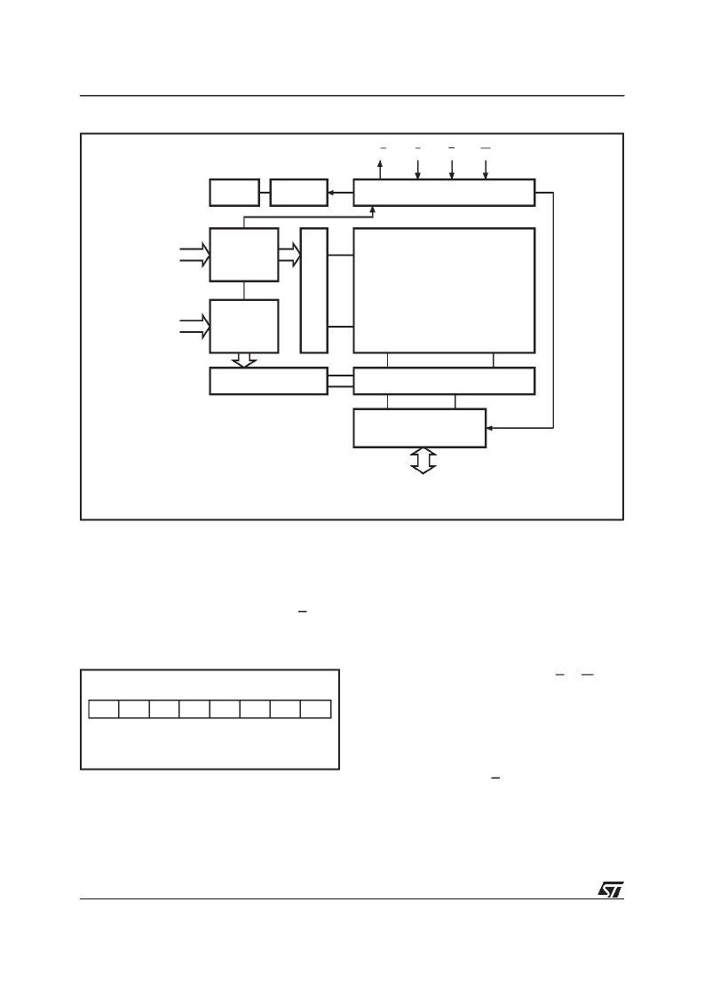
Figure 3. Block Diagram
MicrocontrollerControl Interface
The M28C64C providestwo writeoperationstatus
bitsandonestatuspinthatcanbe usedtominimize
thesystemwritecycle.Thesesignals areavailable
on the I/O port bits DQ7 or DQ6 of the memory
duringprogrammingcycleonly,or asthe RBsignal
on a separate pin.
DQ7
DQ6 DQ5 DQ4 DQ3 DQ2
DQ1 DQ0
DP
TB
PLTS Hi-Z
Hi-Z
Hi-Z
Hi-Z
Hi-Z
Figure 4. StatusBit Assignment
DP = Data Polling
TB = Toggle Bit
PLTS = Page Load Timer Status
Data Polling bit (DQ7).
During the internal write
cycle, any attempt to read the last byte written will
produce on DQ7 the complementary value of the
previously latched bit. Once the write cycle is fin-
ished the true logic value appears on DQ7 in the
read cycle.
Toggle bit (DQ6).
The M28C64C offers another
way for determining when the internal write cycle
iscompleted.DuringtheinternalErase/Writecycle,
DQ6 will toggle from ”0” to ”1” and ”1” to ”0” (the
first read value is ”0”) on subsequent attempts to
readanyaddressin thememory.Whenthe internal
cycle is completed the toggling will stop and the
device will be accessible for a new Read or Write
operation.
Page Load Timer Status bit (DQ5)
. In the Page
Write mode data may be latched by E or W up to
100
μ
s after the previous byte.Up to 32 bytes may
be input. The Data output (DQ5) indicates the
status of the internal Page Load Timer. DQ5 may
be read by asserting Output Enable Low (t
PLTS
).
DQ5 Low indicates the timer is running,
indicates time-out after which the write cycle will
start and no new datamay be input.
Ready/Busy pin.
The RB pin provides a signal at
its open drain output which is low during the
erase/write cycle, but which is released at the
completionof the programming cycle.
High
4/15
M28C64C, M28C64X
相關(guān)PDF資料 |
PDF描述 |
|---|---|
| M28C64X-150MS1 | 64 Kbit 8Kb x8 Parallel EEPROM |
| M28C64X-150P6 | 64 Kbit 8Kb x8 Parallel EEPROM |
| M28C64X-150P1 | 64 Kbit 8Kb x8 Parallel EEPROM |
| M28C64X-150N6 | 64 Kbit 8Kb x8 Parallel EEPROM |
| M28C64X-150N1 | 64 Kbit 8Kb x8 Parallel EEPROM |
相關(guān)代理商/技術(shù)參數(shù) |
參數(shù)描述 |
|---|---|
| M28C64X-150MS1 | 制造商:STMICROELECTRONICS 制造商全稱:STMicroelectronics 功能描述:64 Kbit 8Kb x8 Parallel EEPROM |
| M28C64X-150MS6 | 制造商:STMICROELECTRONICS 制造商全稱:STMicroelectronics 功能描述:64 Kbit 8Kb x8 Parallel EEPROM |
| M28C64X-150N1 | 制造商:STMICROELECTRONICS 制造商全稱:STMicroelectronics 功能描述:64 Kbit 8Kb x8 Parallel EEPROM |
| M28C64X-150N6 | 制造商:STMICROELECTRONICS 制造商全稱:STMicroelectronics 功能描述:64 Kbit 8Kb x8 Parallel EEPROM |
| M28C64X-150P1 | 制造商:STMICROELECTRONICS 制造商全稱:STMicroelectronics 功能描述:64 Kbit 8Kb x8 Parallel EEPROM |
發(fā)布緊急采購,3分鐘左右您將得到回復(fù)。