- 您現(xiàn)在的位置:買賣IC網(wǎng) > PDF目錄358973 > M24M01S-LA6T (意法半導(dǎo)體) 5015 RR 26#16 PIN RECP PDF資料下載
參數(shù)資料
| 型號: | M24M01S-LA6T |
| 廠商: | 意法半導(dǎo)體 |
| 英文描述: | 5015 RR 26#16 PIN RECP |
| 中文描述: | 1兆位串行IC總線的EEPROM |
| 文件頁數(shù): | 3/19頁 |
| 文件大小: | 120K |
| 代理商: | M24M01S-LA6T |

3/19
M24M01
SIGNAL DESCRIPTION
Serial Clock (SCL)
This input signal is used to strobe all data in and
out of the device. In applications where this signal
is used by slave devices to synchronize the bus to
a slower clock, the bus master must have an open
drain output, and a pull-up resistor must be con-
nected from Serial Clock (SCL) to V
CC
. (Figure 4
indicates how the value of the pull-up resistor can
be calculated). In most applications, though, this
method of synchronization is not employed, and
so the pull-up resistor is not necessary, provided
that the bus master has a push-pull (rather than
open drain) output.
Serial Data (SDA)
This bi-directional signal is used to transfer data in
or out of the device. It is an open drain output that
may be wire-OR’ed with other open drain or open
collector signals on the bus. A pull up resistor must
be connected from Serial Data (SDA) to V
CC
. (Fig-
ure 4 indicates how the value of the pull-up resistor
can be calculated).
Chip Enable (E1, E2)
These input signals are used to set the value that
is to be looked for on bits b3 and b2 of the 7-bit De-
vice Select Code. These inputs must be tied to
V
CC
or V
SS
, to establish the Device Select Code.
When unconnected, the Chip Enable (E1, E2) sig-
nals are internally read as V
IL
(see Tables 10 and
11).
Write Control (WC)
This input signal is useful for protecting the entire
contents of the memory from inadvertent write op-
erations. Write operations are disabled to the en-
tire memory array when Write Control (WC) is
driven High. When unconnected, the signal is in-
ternally read as V
IL
, and Write operations are al-
lowed.
When Write Control (WC) is driven High, Device
Select and Address bytes are acknowledged,
Data bytes are not acknowledged.
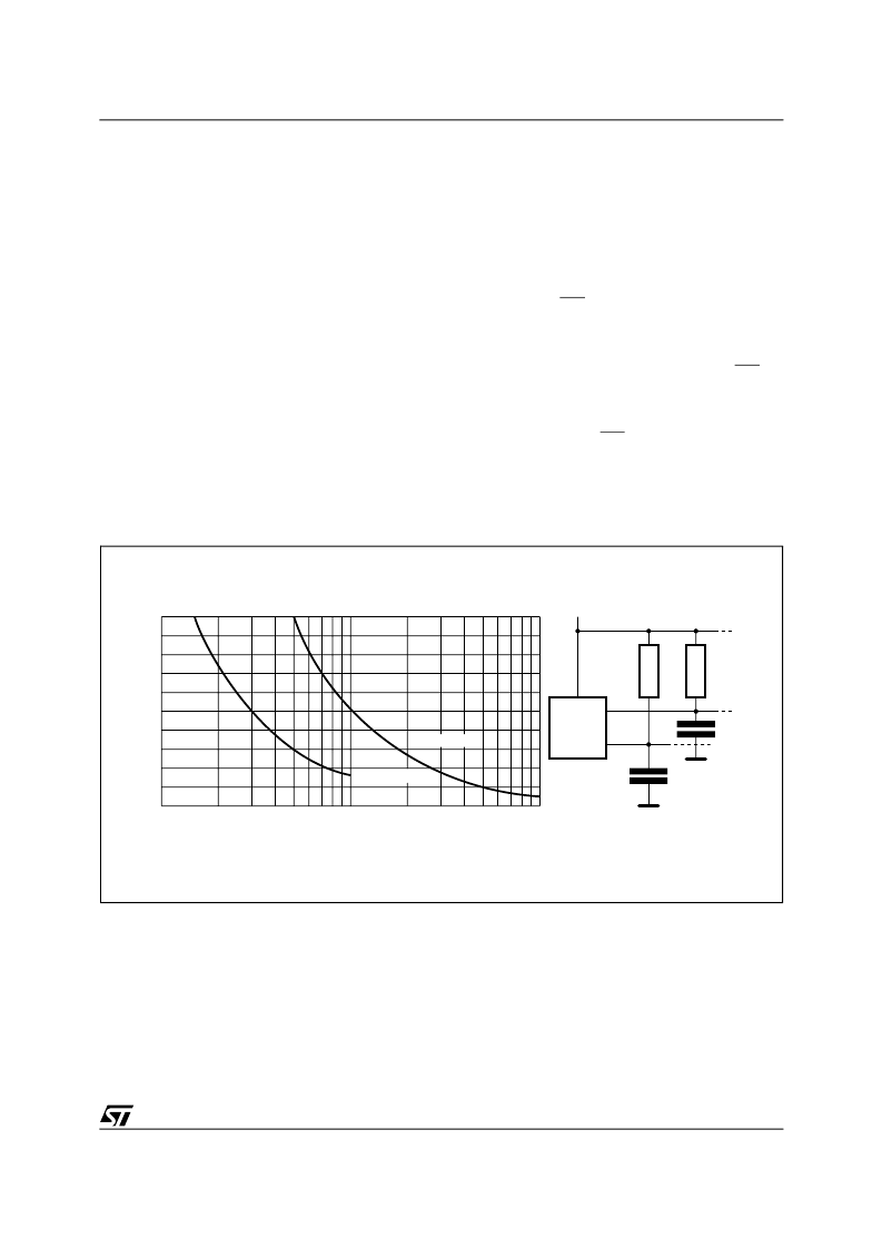
Figure 4. Maximum R
L
Value versus Bus Capacitance (C
BUS
) for an I
2
C Bus
AI01665
VCC
CBUS
SDA
RL
MASTER
RL
SCL
CBUS
100
0
4
8
12
16
20
CBUS (pF)
M
)
10
1000
fc = 400kHz
fc = 100kHz
相關(guān)PDF資料 |
PDF描述 |
|---|---|
| M24M01V-LA6T | 1 Mbit Serial IC Bus EEPROM |
| M24M01-V | 1 Mbit Serial IC Bus EEPROM |
| M24M01-S | 1 Mbit Serial IC Bus EEPROM |
| M24M01 | 1 Mbit Serial IC Bus EEPROM |
| M25P64-VME6 | 4 Mbit Uniform Sector, Serial Flash Memory |
相關(guān)代理商/技術(shù)參數(shù) |
參數(shù)描述 |
|---|---|
| M24M01-V | 制造商:STMICROELECTRONICS 制造商全稱:STMicroelectronics 功能描述:1 Mbit Serial IC Bus EEPROM |
| M24M01V-LA6T | 制造商:STMICROELECTRONICS 制造商全稱:STMicroelectronics 功能描述:1 Mbit Serial IC Bus EEPROM |
| M24M01-W | 制造商:STMICROELECTRONICS 制造商全稱:STMicroelectronics 功能描述:1 Mbit serial I?2C bus EEPROM |
| M24M01-WCS3G/A | 制造商:STMICROELECTRONICS 制造商全稱:STMicroelectronics 功能描述:1 Mbit serial I2C bus EEPROM |
| M24M01-WCS3P/A | 制造商:STMICROELECTRONICS 制造商全稱:STMicroelectronics 功能描述:1 Mbit serial I2C bus EEPROM |
發(fā)布緊急采購,3分鐘左右您將得到回復(fù)。