- 您現(xiàn)在的位置:買賣IC網(wǎng) > PDF目錄296343 > M2050-13I666.5143 (INTEGRATED DEVICE TECHNOLOGY INC) VOLTAGE CONTROLLED CLOCK SAW OSCILLATOR, 666.5143 MHz PDF資料下載
參數(shù)資料
| 型號(hào): | M2050-13I666.5143 |
| 廠商: | INTEGRATED DEVICE TECHNOLOGY INC |
| 元件分類: | XO, clock |
| 英文描述: | VOLTAGE CONTROLLED CLOCK SAW OSCILLATOR, 666.5143 MHz |
| 封裝: | LEADLESS, CERAMIC PACKAGE-36 |
| 文件頁(yè)數(shù): | 11/12頁(yè) |
| 文件大小: | 504K |
| 代理商: | M2050-13I666.5143 |
M2050/51/52 Datasheet Rev 1.0
8 of 12
Revised 23Jun2005
Integrate d Circu it Systems, Inc. ● Communications Modules ● www.ics t.com ● tel (508) 852-5400
M2050/51/52
SAW PLL FOR 10GBE 64B/66B FEC
Preliminar y In f o r m atio n
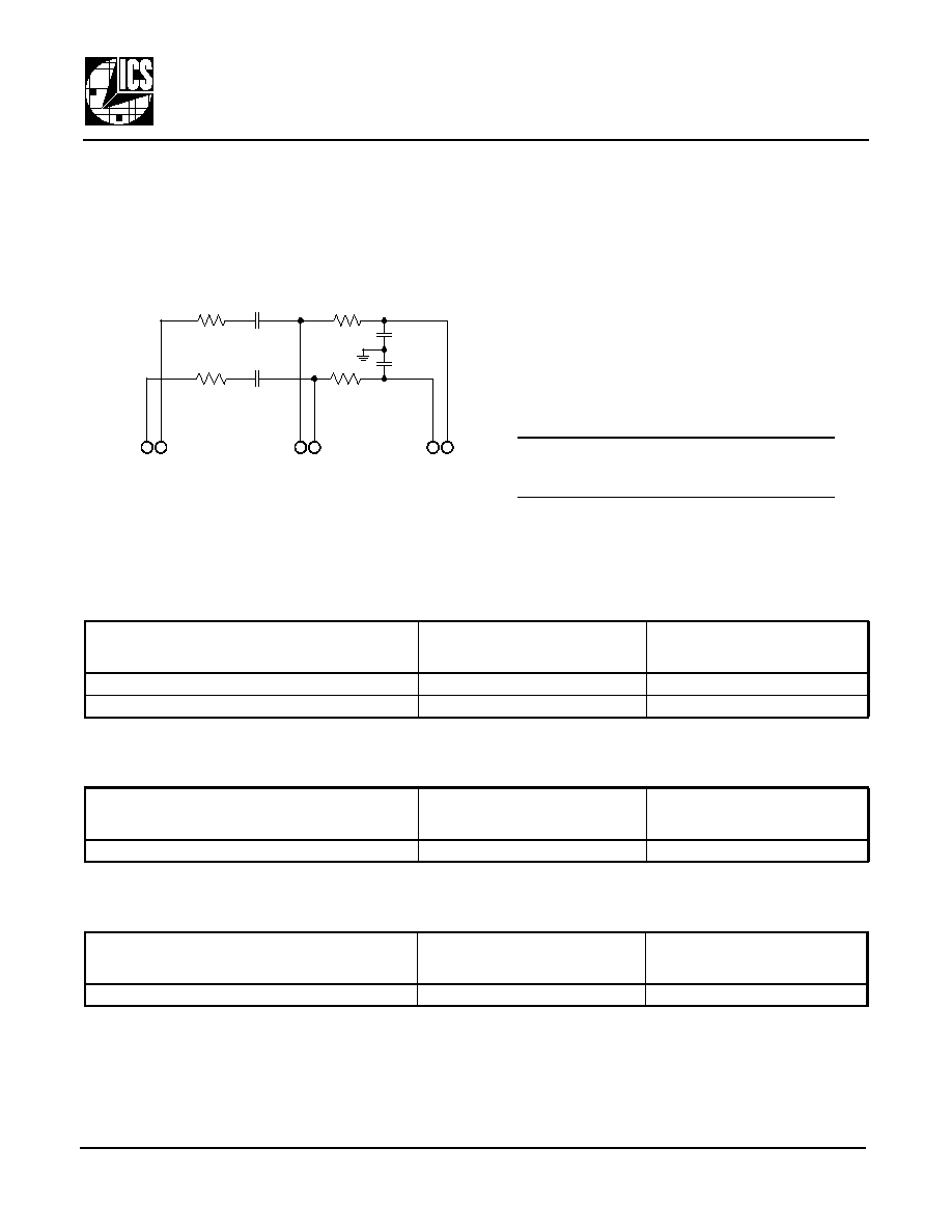
External Loop Filter
To provide stable PLL operation, the M2050/51/52
requires the use of an external loop filter. This is
provided via the provided filter pins (see Figure 5).
Due to the differential signal path design, the
implementation requires two identical complementary
RC filters as shown here.
Figure 5: External Loop Filter
PLL bandwidth is affected by the “Mfec” value and the
“Mfin” value, as well as the VCSO frequency. The
FEC_SEL
setting can be used to actively change PLL loop
bandwidth in a given application. See “Mfec and Rfec
See Tables 9, 10, and 11, Example External Loop Filter
PLL Simulator Tool Available
for additional product information.
C
POST
C
POST
VC
nVC
R
POST
nOP_OUT
OP_OUT
R
POST
R
LOOP
R
LOOP
C
LOOP
C
LOOP
OP_IN
nOP_IN
Example External Loop Filter Component Values
for M2050-11-644.5313 and M2050-11-669.6429
VCSO Parameters: KVCO = 800kHz/V, RIN = 100k (pin NBW = 0), VCSO Bandwidth = 700kHz.
Device Configuration
Example Loop Filter Component Values
Nominal Performance With Values
F Ref
(MHz)
F VCSO
(MHz)
FIN_
FEC_
... SEL1:0
Mfin M R
Phase Det.
Freq. (MHz)
R Loop
C Loop
R Post
C Post
PLL Loop
Bandwidth
Damping
Factor
Passband
Peaking (dB)
Post Filter
Bandwidth
125.00
644.5313 0 1 0 0 5 33 32
3.9063
61.9k
1.0F 59.0k 1000pF 577Hz 6.8
0.043
2.7kHz
125.00
669.6429 0 1 1 0 5 15 14
8.9286
44.2k
1.0F 38.3k 1000pF 908Hz 7.2
0.039
4.1kHz
Example External Loop Filter Component Values
for M2051-11-625.0000
VCSO Parameters: KVCO = 800kHz/V, RIN = 100k (pin NBW = 0), VCSO Bandwidth = 700kHz.
Device Configuration
Example Loop Filter Component Values
Nominal Performance With Values
F Ref
(MHz)
F VCSO
(MHz)
FIN_
FEC_
...SEL1:0
Mfin M R
Phase Det.
Freq. (MHz)
R Loop
C Loop
R Post
C Post
PLL Loop
Bandwidth
Damping
Factor
Passband
Peaking (dB)
Post Filter
Bandwidth
644.5313 625.0000 1 1 0 0
32 33 19.5313
28.0k
1.0F 15.0k 1000pF 1.25kHz 7.0
0.04
10.6kHz
Example External Loop Filter Component Values1
for M2052-11-644.5313
VCSO Parameters: KVCO = 800kHz/V, RIN = 100k (pin NBW = 0), VCSO Bandwidth = 700kHz.
Device Configuration
Example Loop Filter Component Values
Nominal Performance With Values
F Ref
(MHz)
F VCSO
(MHz)
FIN_
FEC_
...SEL1:0
Mfin M R
Phase Det.
Freq. (MHz)
R Loop
C Loop
R Post
C Post
PLL Loop
Bandwidth
Damping
Factor
Passband
Peaking (dB)
Post Filter
Bandwidth
693.4830 644.5313 1 1 0 0 1 79 85
8.1586
51.0k
1.0F 33.2k 1000pF 986Hz 8.1
0.031
4.8kHz
Note 1: K
VCO , VCSO Bandwidth, Mfin x Mfec Divider Value, and External Loop Filter Component Values determine Loop Bandwidth, Damping
Factor, and Passband Peaking. For PLL Simulator software, go to www.icst.com.
相關(guān)PDF資料 |
PDF描述 |
|---|---|
| M2050-13I669.6429 | VOLTAGE CONTROLLED CLOCK SAW OSCILLATOR, 669.6429 MHz |
| M2050-13I670.8386 | VOLTAGE CONTROLLED CLOCK SAW OSCILLATOR, 670.8386 MHz |
| M2050-13I690.5692 | VOLTAGE CONTROLLED CLOCK SAW OSCILLATOR, 690.5692 MHz |
| M2050-13IFREQ | VOLTAGE CONTROLLED CLOCK SAW OSCILLATOR, 15 MHz - 700 MHz |
| M2051-11-669.3266 | VOLTAGE CONTROLLED CLOCK SAW OSCILLATOR, 669.3266 MHz |
相關(guān)代理商/技術(shù)參數(shù) |
參數(shù)描述 |
|---|---|
| M2050HCZ10 | 制造商:n/a 功能描述:Ships in 2 days |
| M2051 | 制造商:ICS 制造商全稱:ICS 功能描述:SAW PLL FOR 10GBE 64B/66B FEC |
| M2051-11-625.0000 | 制造商:Integrated Device Technology Inc 功能描述:PLL Single 36-Pin CLCC 制造商:Integrated Device Technology Inc 功能描述:FREQUENCY TRANSLATOR |
| M2051-11-625.0000T | 功能描述:時(shí)鐘合成器/抖動(dòng)清除器 FREQUENCY TRANSLATOR RoHS:否 制造商:Skyworks Solutions, Inc. 輸出端數(shù)量: 輸出電平: 最大輸出頻率: 輸入電平: 最大輸入頻率:6.1 GHz 電源電壓-最大:3.3 V 電源電壓-最小:2.7 V 封裝 / 箱體:TSSOP-28 封裝:Reel |
| M2051-11I625.0000 | 制造商:ICS 制造商全稱:ICS 功能描述:SAW PLL FOR 10GBE 64B/66B FEC |
發(fā)布緊急采購(gòu),3分鐘左右您將得到回復(fù)。