- 您現(xiàn)在的位置:買(mǎi)賣(mài)IC網(wǎng) > PDF目錄4402 > M1A3PE1500-PQG208I (Microsemi SoC)IC FPGA 1KB FLASH 1.5M 208-PQFP PDF資料下載
參數(shù)資料
| 型號(hào): | M1A3PE1500-PQG208I |
| 廠商: | Microsemi SoC |
| 文件頁(yè)數(shù): | 107/162頁(yè) |
| 文件大?。?/td> | 0K |
| 描述: | IC FPGA 1KB FLASH 1.5M 208-PQFP |
| 標(biāo)準(zhǔn)包裝: | 24 |
| 系列: | ProASIC3E |
| RAM 位總計(jì): | 276480 |
| 輸入/輸出數(shù): | 147 |
| 門(mén)數(shù): | 1500000 |
| 電源電壓: | 1.425 V ~ 1.575 V |
| 安裝類(lèi)型: | 表面貼裝 |
| 工作溫度: | -40°C ~ 85°C |
| 封裝/外殼: | 208-BFQFP |
| 供應(yīng)商設(shè)備封裝: | 208-PQFP(28x28) |
第1頁(yè)第2頁(yè)第3頁(yè)第4頁(yè)第5頁(yè)第6頁(yè)第7頁(yè)第8頁(yè)第9頁(yè)第10頁(yè)第11頁(yè)第12頁(yè)第13頁(yè)第14頁(yè)第15頁(yè)第16頁(yè)第17頁(yè)第18頁(yè)第19頁(yè)第20頁(yè)第21頁(yè)第22頁(yè)第23頁(yè)第24頁(yè)第25頁(yè)第26頁(yè)第27頁(yè)第28頁(yè)第29頁(yè)第30頁(yè)第31頁(yè)第32頁(yè)第33頁(yè)第34頁(yè)第35頁(yè)第36頁(yè)第37頁(yè)第38頁(yè)第39頁(yè)第40頁(yè)第41頁(yè)第42頁(yè)第43頁(yè)第44頁(yè)第45頁(yè)第46頁(yè)第47頁(yè)第48頁(yè)第49頁(yè)第50頁(yè)第51頁(yè)第52頁(yè)第53頁(yè)第54頁(yè)第55頁(yè)第56頁(yè)第57頁(yè)第58頁(yè)第59頁(yè)第60頁(yè)第61頁(yè)第62頁(yè)第63頁(yè)第64頁(yè)第65頁(yè)第66頁(yè)第67頁(yè)第68頁(yè)第69頁(yè)第70頁(yè)第71頁(yè)第72頁(yè)第73頁(yè)第74頁(yè)第75頁(yè)第76頁(yè)第77頁(yè)第78頁(yè)第79頁(yè)第80頁(yè)第81頁(yè)第82頁(yè)第83頁(yè)第84頁(yè)第85頁(yè)第86頁(yè)第87頁(yè)第88頁(yè)第89頁(yè)第90頁(yè)第91頁(yè)第92頁(yè)第93頁(yè)第94頁(yè)第95頁(yè)第96頁(yè)第97頁(yè)第98頁(yè)第99頁(yè)第100頁(yè)第101頁(yè)第102頁(yè)第103頁(yè)第104頁(yè)第105頁(yè)第106頁(yè)當(dāng)前第107頁(yè)第108頁(yè)第109頁(yè)第110頁(yè)第111頁(yè)第112頁(yè)第113頁(yè)第114頁(yè)第115頁(yè)第116頁(yè)第117頁(yè)第118頁(yè)第119頁(yè)第120頁(yè)第121頁(yè)第122頁(yè)第123頁(yè)第124頁(yè)第125頁(yè)第126頁(yè)第127頁(yè)第128頁(yè)第129頁(yè)第130頁(yè)第131頁(yè)第132頁(yè)第133頁(yè)第134頁(yè)第135頁(yè)第136頁(yè)第137頁(yè)第138頁(yè)第139頁(yè)第140頁(yè)第141頁(yè)第142頁(yè)第143頁(yè)第144頁(yè)第145頁(yè)第146頁(yè)第147頁(yè)第148頁(yè)第149頁(yè)第150頁(yè)第151頁(yè)第152頁(yè)第153頁(yè)第154頁(yè)第155頁(yè)第156頁(yè)第157頁(yè)第158頁(yè)第159頁(yè)第160頁(yè)第161頁(yè)第162頁(yè)
ProASIC3E Flash Family FPGAs
Revision 13
2-35
1.5 V LVCMOS (JESD8-11)
Low-Voltage CMOS for 1.5 V is an extension of the LVCMOS standard (JESD8-5) used for general-
purpose 1.5 V applications. It uses a 1.5 V input buffer and a push-pull output buffer.
Table 2-41 Minimum and Maximum DC Input and Output Levels
1.5 V
LVCMOS
VIL
VIH
VOL
VOH
IOL IOH IOSL
IOSH IIL1 IIH2
Drive
Strength
Min.
V
Max.
V
Min.
V
Max.
V
Max.
V
Min.
VmA mA
Max.
mA3
Max.
mA3 A4 A4
2 mA
–0.3 0.30 * VCCI 0.7 * VCCI
3.6
0.25 * VCCI
0.75 * VCCI
2
16
13
10 10
4 mA
–0.3 0.30 * VCCI 0.7 * VCCI
3.6
0.25 * VCCI
0.75 * VCCI
4
33
25
10 10
6 mA
–0.3 0.30 * VCCI 0.7 * VCCI
3.6
0.25 * VCCI
0.75 * VCCI
6
39
32
10 10
8 mA
–0.3 0.30 * VCCI 0.7 * VCCI
3.6
0.25 * VCCI
0.75 * VCCI
8
55
66
10 10
12 mA
–0.3 0.30 * VCCI 0.7 * VCCI
3.6
0.25 * VCCI
0.75 * VCCI
12 12
55
66
10 10
Notes:
1. IIL is the input leakage current per I/O pin over recommended operation conditions where –0.3 V< VIN < VIL.
2. IIH is the input leakage current per I/O pin over recommended operating conditions VIH < VIN < VCCI. Input current is
larger when operating outside recommended ranges.
3. Currents are measured at high temperature (100°C junction temperature) and maximum voltage.
4. Currents are measured at 85°C junction temperature.
5. Software default selection highlighted in gray.
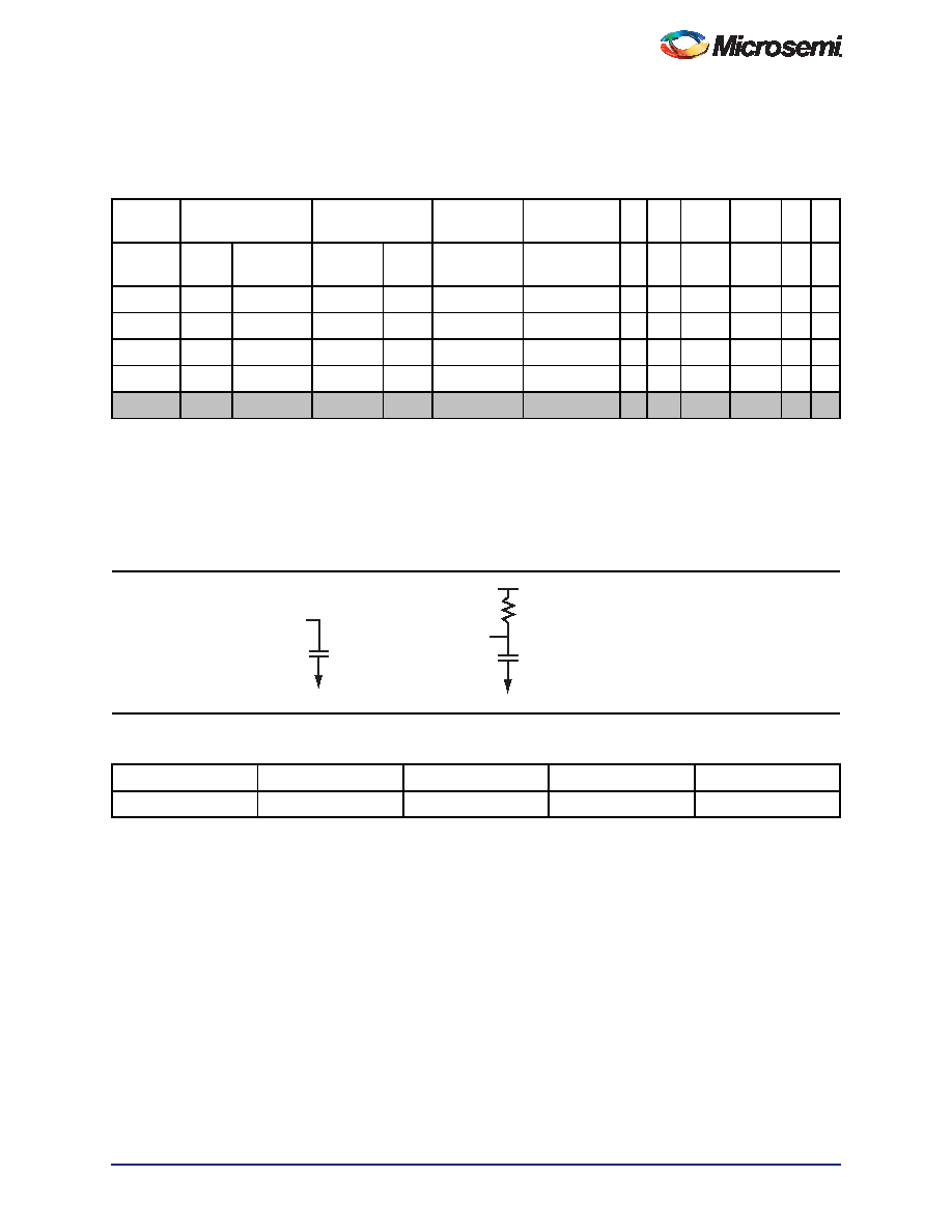
Figure 2-10 AC Loading
Table 2-42 AC Waveforms, Measuring Points, and Capacitive Loads
Input Low (V)
Input High (V)
Measuring Point* (V)
VREF (typ.) (V)
CLOAD (pF)
0
1.5
0.75
–
35
Note: *Measuring point = Vtrip. See Table 2-15 on page 2-18 for a complete table of trip points.
Test Point
Enable Path
Datapath
35 pF
R = 1 k
R to VCCI for tLZ / tZL / tZLS
R to GND for tHZ / tZH / tZHS
35 pF for tZH / tZHS / tZL / tZLS
35 pF for tHZ / tLZ
相關(guān)PDF資料 |
PDF描述 |
|---|---|
| A3PE1500-PQG208I | IC FPGA 1KB FLASH 1.5M 208-PQFP |
| APA450-BG456I | IC FPGA PROASIC+ 450K 456-PBGA |
| APA450-BGG456I | IC FPGA PROASIC+ 450K 456-PBGA |
| A54SX72A-1PQG208I | IC FPGA SX-A 108K 208-PQFP |
| A54SX72A-1PQ208I | IC FPGA SX-A 108K 208-PQFP |
相關(guān)代理商/技術(shù)參數(shù) |
參數(shù)描述 |
|---|---|
| M1A3PE1500-PQG896 | 制造商:ACTEL 制造商全稱(chēng):Actel Corporation 功能描述:ProASIC3E Flash Family FPGAs |
| M1A3PE1500-PQG896ES | 制造商:ACTEL 制造商全稱(chēng):Actel Corporation 功能描述:ProASIC3E Flash Family FPGAs |
| M1A3PE1500-PQG896I | 制造商:ACTEL 制造商全稱(chēng):Actel Corporation 功能描述:ProASIC3E Flash Family FPGAs |
| M1A3PE1500-PQG896PP | 制造商:ACTEL 制造商全稱(chēng):Actel Corporation 功能描述:ProASIC3E Flash Family FPGAs |
| M1A3PE3000-1FG324 | 功能描述:IC FPGA 1KB FLASH 3M 324-FBGA RoHS:否 類(lèi)別:集成電路 (IC) >> 嵌入式 - FPGA(現(xiàn)場(chǎng)可編程門(mén)陣列) 系列:ProASIC3E 產(chǎn)品培訓(xùn)模塊:Three Reasons to Use FPGA's in Industrial Designs Cyclone IV FPGA Family Overview 特色產(chǎn)品:Cyclone? IV FPGAs 標(biāo)準(zhǔn)包裝:60 系列:CYCLONE® IV GX LAB/CLB數(shù):9360 邏輯元件/單元數(shù):149760 RAM 位總計(jì):6635520 輸入/輸出數(shù):270 門(mén)數(shù):- 電源電壓:1.16 V ~ 1.24 V 安裝類(lèi)型:表面貼裝 工作溫度:0°C ~ 85°C 封裝/外殼:484-BGA 供應(yīng)商設(shè)備封裝:484-FBGA(23x23) |
發(fā)布緊急采購(gòu),3分鐘左右您將得到回復(fù)。