- 您現(xiàn)在的位置:買賣IC網(wǎng) > PDF目錄369882 > LXE1686-02 CCFL Inverter Module - Single Lamp PDF資料下載
參數(shù)資料
| 型號(hào): | LXE1686-02 |
| 英文描述: | CCFL Inverter Module - Single Lamp |
| 中文描述: | CCFL逆變器模塊-單燈 |
| 文件頁(yè)數(shù): | 4/6頁(yè) |
| 文件大小: | 131K |
| 代理商: | LXE1686-02 |

LXE1684
Evaluation Board Installation Guide
Copyright 2001
Rev. 0.1 9/11/01
Page 4
New Product Information
W
M
.
C
MOSFET Selection
The top and bottom FETs
MUST
be Logic level MOSFETs. For a 12V power input application the total
gate capacitance of each MOSFET should be less than 50nC. This is due to the fact that SOIC-14 package
has a junction to ambient temperature coefficient of 165°C per Watt. Maximum V
DS
rating of MOSFETs
for 12V operation should be at least 30V.
The LXE1684 can accommodate Top and Bottom MOSFETs with both through hole and surface mount
footprints such as TO-220, SMD220, TO-263,TO-252, SOT-223 such as the Vishay Logic MOSFET
SUB45N05-20L.
Please refer to LX1684 data sheet for MOSFET selections. For 12V application, care must be taken in
selecting MOSFET to make sure that LX1684 junction temperature is within acceptable limits. Die
temperature should be less than 125°C.
For 12V to 3.3V application
,
the current flow through the bottom MOSFET is more than twice the current
flow through the top MOSFET. The power supply designer therefore should choose a larger MOSFET
and larger heat sink for the bottom MOSFET. Please refer to LX1684 data sheet for calculation of power
dissipation on the top and bottom MOSFETs.
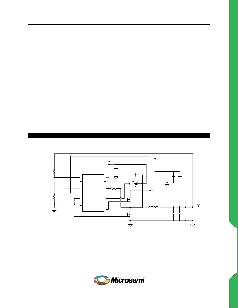
LXE1684 Evaluation Board Schematic
FB
NC
SS
CSP
GND
PGND
BDR
TDR
NC
VC1
NC
CS
NC
VCC
Css
0.1μF
R2
100 Ohm
R1
162 Ohm
C5
1μF
5V 5%
V
IN
Controller
RSET
3.3K
L1
10μF
Q2
SUB45N05-
20L
3x
820μF,
16V
Q1
SUB45N
05-20L
12V 10% V
IN
Power*
C1
0.1μF
3.3V
10A
5817SMT
C4,C4A,C4B
L1 is a powdered
iron toroid
1
2
3
4
5
6
7
14
13
12
11
10
9
8
D1A0
VOUT
C3B,C,D,E
4x
1500μF
6.3V
V
OUT
= V
REF
(1+R1/R2)
*V
can be reconfigured to any voltage between 3V and 13.2V. This change
may require different a input/output capacitance and changes to the output
voltage divider resistors, etc, see data sheet.
L
X
E
1
6
8
4
U
S
E
R
G
U
I
D
E
相關(guān)PDF資料 |
PDF描述 |
|---|---|
| LXE1686-03 | CCFL Inverter Module - Single Lamp |
| LXE1810-100EVALKIT | Thermo Electric Controller IC |
| LXE1810-50EVALKIT | Thermo Electric Controller IC |
| LXE1810EVALKIT | Thermo Electric Controller IC |
| LXL111G | |
相關(guān)代理商/技術(shù)參數(shù) |
參數(shù)描述 |
|---|---|
| LXE1686-03 | 制造商:未知廠家 制造商全稱:未知廠家 功能描述:CCFL Inverter Module - Single Lamp |
| LXE1686-0X | 制造商:MICROSEMI 制造商全稱:Microsemi Corporation 功能描述:INVERTER EVALUATION BOARD |
| LXE1686-OX | 制造商:MICROSEMI 制造商全稱:Microsemi Corporation 功能描述:INVERTER EVALUATION BOARD |
| LXE1710 | 制造商:MICROSEMI 制造商全稱:Microsemi Corporation 功能描述:EVALUATION KIT |
| LXE1710HV | 制造商:Microsemi Corporation 功能描述:AUDIOMAX EVALUATION KIT |
發(fā)布緊急采購(gòu),3分鐘左右您將得到回復(fù)。