- 您現(xiàn)在的位置:買賣IC網(wǎng) > PDF目錄69008 > LX2206ILD-TR (MICROSEMI CORP-ANALOG MIXED SIGNAL GROUP) 1-CHANNEL POWER SUPPLY SUPPORT CKT, PDSO10 PDF資料下載
參數(shù)資料
| 型號: | LX2206ILD-TR |
| 廠商: | MICROSEMI CORP-ANALOG MIXED SIGNAL GROUP |
| 元件分類: | 電源管理 |
| 英文描述: | 1-CHANNEL POWER SUPPLY SUPPORT CKT, PDSO10 |
| 封裝: | ROHS COMPLIANT, PLASTIC, MLP-10 |
| 文件頁數(shù): | 7/14頁 |
| 文件大?。?/td> | 296K |
| 代理商: | LX2206ILD-TR |
LX2206
PRODUCTION DATA SHEET
Microsemi
Analog Mixed Signal Group
11861 Western Avenue, Garden Grove, CA. 92841, 714-898-8121, Fax: 714-893-2570
Page 2
Copyright
2007
Rev. 1.3a, 2007-08-28
WWW
.Microse
m
i
.CO
M
Dual Level Lithium Ion Battery Charger
TM
ABSOLUTE MAXIMUM RATINGS
Supply Input Voltage (IN, BAT) ...................................................................... -0.3V to 7V
All other pins ............................................................................................-0.3V to VSUPPLY
Battery Charging Current .............................................................................................1.1A
Operating Temperature Range .........................................................................-40 to 150
°C
Maximum Operating Junction Temperature .............................................................. 150
°C
Storage Temperature Range.........................................................................-65
°C to 150°C
Lead Temperature (Soldering 10 seconds)................................................................. 300
°C
Package Peak Temp. for Solder Reflow (40 seconds maximum exposure) ... 260°C (+0 -5)
Note: Exceeding these ratings could cause damage to the device. All voltages are with respect to
Ground. Currents are positive into, negative out of specified terminal
.
TH ERMAL DATA
LD Plastic Micro Leadframe Package 10-Pin
THERMAL RESISTANCE
-JUNCTION TO AMBIENT,
θ
JA
33
°C/W
Junction Temperature Calculation: TJ = TA + (PD x θJA).
The
θ
JA numbers are guidelines for the thermal performance of the device/pc-board system. All of the
above assume no ambient airflow.
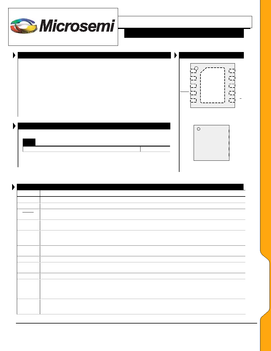
PACKAGE PIN OUT
IN
1
2
3
4
56
7
8
9
10
CONNECT
BOTTOM PAD
TO
GND
STAT
DCOK
SD
H/L
LCP
HCP
TMP
BAT
CMP
LD PACKAGE PINOUT
(Top View)
RoHS / Pb-free 100% matte Tin Pin Finish
220
6
xxx
x
MSC
Part Marking
xxxx = Denotes date and
lot code Identification
`
FUNCTIONAL PIN DESCRIPTION
Name
Description
BAT
Battery – Connect to a single cell Lithium Ion Battery.
CMP
Compensation – Connect the series combination of a 1k resistor and a 0.47F capacitor from CMP to IN.
DCOK
Power status logic pin and LED driver – This pin is an open drain output that can sink 20mA of current to drive an
external LED. This pin is low impedance to GND when the Input voltage is high enough to charge the Battery.
GND
Ground – Connect to the system ground plane. Use sufficient via copper area to allow for thermal conduction
from the IC to the GND plane.
HCP
High Current Programming (and Termination Current Programming) – Connect a resistor to ground to set the
constant current high level. The termination current is set to 1/10 of the High Current Programming Level.
For a value of 19.6K, the High Current is 460mA and the Termination Current is 46mA.
H/L
High or Low load select logic input – A logic high selects the constant charge current level set by the HCP pin
resistor and a logic low selects the constant charge current level set by the LCP pin resistor
IN
Input Power – Connect to a wall adapter or a USB power plug.
LCP
Low Current Programming – Connect a resistor to ground to set the constant current low level.
For a value of 110K, the Low Current is 92mA.
SD
Shutdown – A logic high places the LX2206 in sleep mode; can also be used for USB suspend.
STAT
Charging status logic pin and LED driver – This pin can source or sink 10mA of current to drive an external LED
in either output state. This pin is low (current sinking mode) when the battery is in charging mode and becomes
high (current sourcing mode) when the charge cycle is finished. It becomes a high impedance when the input
power is removed.
TMP
Battery Temperature Monitor – This sense pin determines the battery temperature for charging out of
temperature range lockout and is connected to a resistor network as defined in the Applications section. The
TMP pin is grounded if this function is not used.
PP
AA
CC
KK
AA
GG
EE
DD
AA
TT
AA
相關PDF資料 |
PDF描述 |
|---|---|
| LYPR540AH | SPECIALTY ANALOG CIRCUIT, PBGA28 |
| LZ37C1B | SPECIALTY ANALOG CIRCUIT, CQCC36 |
| M0358WC140 | 358 A, 1400 V, SILICON, RECTIFIER DIODE |
| M0358WC120 | 358 A, 1200 V, SILICON, RECTIFIER DIODE |
| M1104NC400 | 1104 A, 4000 V, SILICON, RECTIFIER DIODE |
相關代理商/技術參數(shù) |
參數(shù)描述 |
|---|---|
| LX2207 | 制造商:MICROSEMI 制造商全稱:Microsemi Corporation 功能描述:Three Level Lithium Ion Battery Charger |
| LX2207 EVAL KIT | 制造商:Microsemi Corporation 功能描述:LINEAR - LITHIUM ION - Bulk |
| LX2207_0710 | 制造商:MICROSEMI 制造商全稱:Microsemi Corporation 功能描述:Three Level Lithium Ion Battery Charger |
| LX2207ILD | 制造商:Microsemi Corporation 功能描述:LINEAR - LITHIUM ION - Bulk |
| LX2207ILD-TR | 制造商:MICROSEMI 制造商全稱:Microsemi Corporation 功能描述:Three Level Lithium Ion Battery Charger |
發(fā)布緊急采購,3分鐘左右您將得到回復。