- 您現(xiàn)在的位置:買賣IC網(wǎng) > PDF目錄98004 > LX2203CLD-TR (MICROSEMI CORP-ANALOG MIXED SIGNAL GROUP) 1-CHANNEL POWER SUPPLY SUPPORT CKT, PDSO10 PDF資料下載
參數(shù)資料
| 型號: | LX2203CLD-TR |
| 廠商: | MICROSEMI CORP-ANALOG MIXED SIGNAL GROUP |
| 元件分類: | 電源管理 |
| 英文描述: | 1-CHANNEL POWER SUPPLY SUPPORT CKT, PDSO10 |
| 封裝: | LEAD FREE, PLASTIC, MLP-10 |
| 文件頁數(shù): | 11/11頁 |
| 文件大小: | 186K |
| 代理商: | LX2203CLD-TR |
LX2203
PRODUCTION DATA SHEET
Microsemi
Integrated Products Division
11861 Western Avenue, Garden Grove, CA. 92841, 714-898-8121, Fax: 714-893-2570
Page 9
Copyright
2004
Rev. 1.0, 2005-01-06
WWW
.Microse
m
i
.CO
M
Li-Ion Battery Charger
TM
APPLICATION NOTE (CONTINU E D)
CONSTANT
CHARGE
CURRENT
PROGRAMMING
(CONTINUED)
The table below lists some popular Constant Current
Settings along with the associated CCP pin current and
programming resistor:
Charge Current
Iccp Current
Rccp Value
1.0A
13.75A
90.9K
500mA
6.22A
200K
100mA
1.00A
1200K
It is possible to change the constant current setting by
changing the Rccp resistor while in charge mode. Since the
termination current is independent of the charge current,
lowering the constant charge current will increase the charge
time, but will not reduce the stored charge in the battery at
the charge termination point.
The circuit in Figure 4 is an example of a battery charger
configured to charge at 1A, 500mA or 100mA. The switches
are logically controlled and reduce the resistance at the CCP
pin when switched in. It is possible to eliminate the
MOSFET devices if open drain logic is available.
The logic for the CP1 and CP2 would normally come
from the appliance processor which would need to have the
capability to communicate over the USB interface. If there
is only one power connector and the USB interface is active,
the logic could assume the power was coming from the USB
bus and not the wall adapter. If the USB interface is active,
the USB application will know if the appliance has been
enumerated as a high or low load and would set CP1 and
CP2 appropriately.
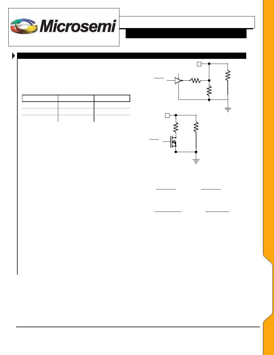
It is possible to change the current programming circuit to
drive it directly with CMOS logic, but this requires that the
CMOS logic power supply be well regulated (+/-2%). Each
switch resistor leg in Figure 4 can be replaced with a two
resistor network tied to the output of a CMOS gate.
1.21M
R1
CCP
R2
Vcc
500mA/100mA
1.21M
243k
CCP
500mA/100mA
Rsw
Figure 6 – Circuits to provide 100mA and 500mA
constant charge currents.
The values of R1 and R2 are selected such that:
25
.
1
R
V
2
1
2
CC
=
+
×
&
SW
2
1
2
1
R
=
+
×
Solving these equations:
25
.
1
R
V
R
SW
CC
1
×
=
&
SW
1
SW
1
2
R
×
=
For Vcc = 3.3V and Rsw = 243k; R1 = 649k; R2 = 392k.
These values should provide charge currents of 100mA and
500mA
.
COMPENSATION CAPACITOR
A compensation capacitor of value 0.01uF is required
between the CMP pin and VIN.
AA
PP
LL
IICC
AA
TT
IIOO
NN
SS
相關(guān)PDF資料 |
PDF描述 |
|---|---|
| LX2203CLD-TR | 1-CHANNEL POWER SUPPLY SUPPORT CKT, PDSO10 |
| LX2207ILD-TR | 1-CHANNEL POWER SUPPLY SUPPORT CKT, PDSO12 |
| LY510ALHTR | SPECIALTY ANALOG CIRCUIT, PBGA16 |
| LZ0P3817 | SPECIALTY ANALOG CIRCUIT, CQCC36 |
| M0280RJ240 | 123 A, 2400 V, SILICON, RECTIFIER DIODE |
相關(guān)代理商/技術(shù)參數(shù) |
參數(shù)描述 |
|---|---|
| LX2205 | 制造商:MICROSEMI 制造商全稱:Microsemi Corporation 功能描述:1A Li-Ion Battery Charger with Power Source Management |
| LX2205 EVAL KIT | 制造商:Microsemi Corporation 功能描述:LINEAR - LITHIUM ION - Bulk |
| LX2205ILQ | 制造商:Microsemi Corporation 功能描述:LINEAR - LITHIUM ION - Bulk |
| LX2206 | 制造商:MICROSEMI 制造商全稱:Microsemi Corporation 功能描述:Dual Level Lithium Ion Battery Charger |
| LX2206 EVAL KIT | 制造商:Microsemi Corporation 功能描述:LINEAR - LITHIUM ION - Bulk |
發(fā)布緊急采購,3分鐘左右您將得到回復(fù)。