- 您現(xiàn)在的位置:買賣IC網(wǎng) > PDF目錄30778 > LX1708ILQ-TR (MICROSEMI CORP-ANALOG MIXED SIGNAL GROUP) 15 W, 2 CHANNEL, AUDIO AMPLIFIER, PQCC32 PDF資料下載
參數(shù)資料
| 型號: | LX1708ILQ-TR |
| 廠商: | MICROSEMI CORP-ANALOG MIXED SIGNAL GROUP |
| 元件分類: | 音頻/視頻放大 |
| 英文描述: | 15 W, 2 CHANNEL, AUDIO AMPLIFIER, PQCC32 |
| 封裝: | 7 X 7 MM, ROHS COMPLIANT, PLASTIC, MLPQ-32 |
| 文件頁數(shù): | 2/17頁 |
| 文件大小: | 390K |
| 代理商: | LX1708ILQ-TR |

LX1708
PRODUCTION DATA SHEET
Microsemi
Analog Mixed Signal Group
11861 Western Avenue, Garden Grove, CA. 92841, 714-898-8121, Fax: 714-893-2570
Page 10
Copyright
2007
Rev. 1.3, 2007-04-05
WWW
.Microse
m
i
.CO
M
15+15W Stereo Filterless Class-D Amplifier
TM
APPLICATION NOTE/PCB DESIGN GUID E LIN E
OSCILLATOR
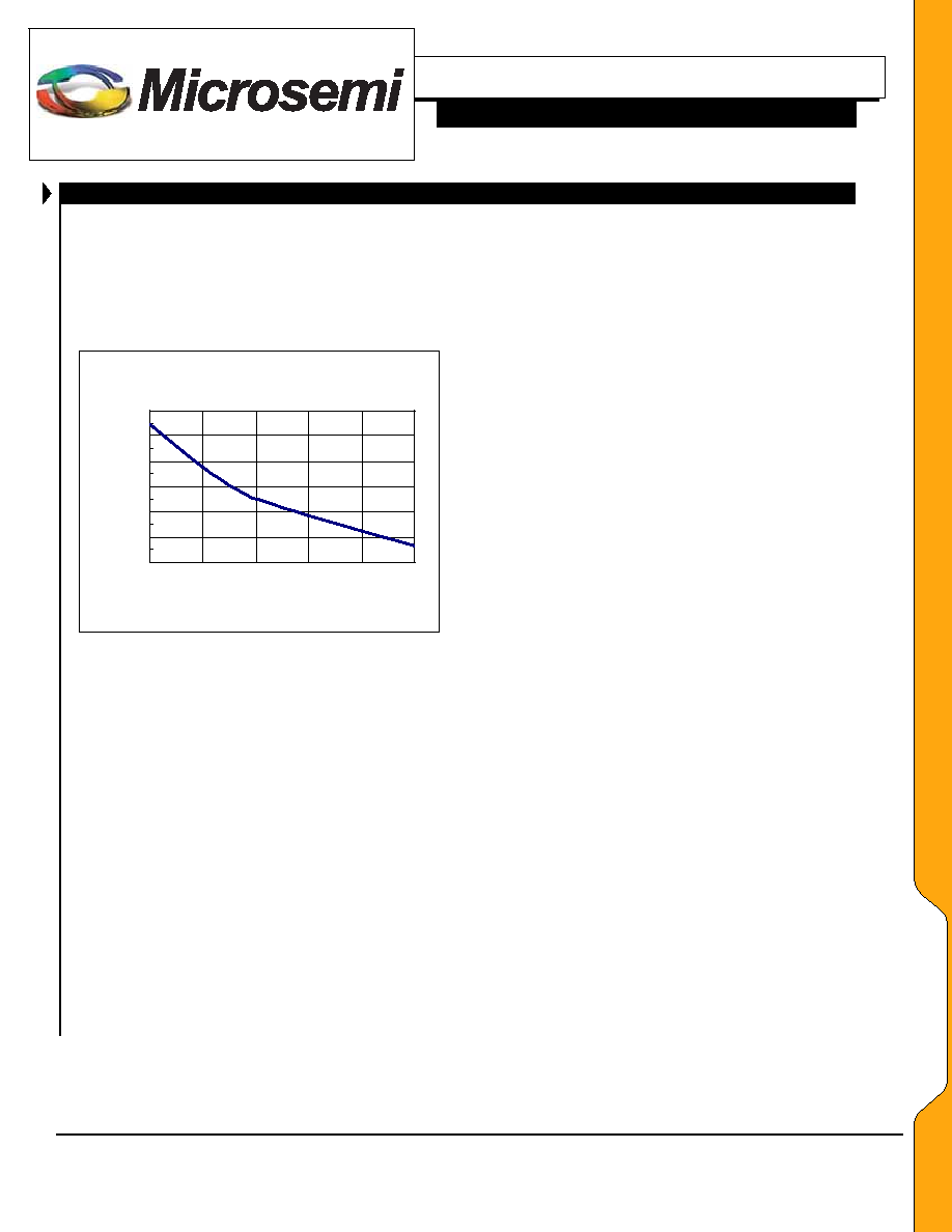
The value of ROSC selects the switching frequency;
smaller values increase the switching frequency.
See
Figure 4, Typical Switching Frequency vs. ROSC. The
recommended range of ROSC is between 17.5K and
42.5K
Sw itching Frequency vs ROSC
150
200
250
300
350
400
450
17.5
22.5
27.5
32.5
37.5
42.5
ROSC (kOhm s)
SW
F
R
EQ
(k
H
z
)
Figure 4 – Typical Switching Frequency vs. ROSC
BOOTSTRAP CAPACITORS
C8, C9, C14, and C15 are bootstrap capacitors for
internal NMOSFETs gate drive voltage, they work together
with internal diodes to provide sufficient gate drive voltage
for upper MOSFETS. Those capacitors should be placed as
close to the IC as possible.
BYPASSING CAPACITORS
C7, C10, C11, C12, C13, and C16 are bypassing
capacitors for input supplies and internal reference voltage
(VREF), nominal value is 1F. These capacitors should be
placed as close to the IC as possible, to guarantee low ripple
and noise.
PCB DESIGN GUIDELINES
Component placement for the LX1708 should be done
such that low-level inputs to the LX1708 are routed away
from the high frequency switching outputs. Special care
should be given to the bypass and bootstrap capacitors.
Capacitors (C7, C10, C13, C16, C8, C9, C14, and C15 in
the application schematic), should be placed as close to the
IC as possible. If workable, they should be mounted on the
same layer as the IC, with a direct connection to the IC on
that layer. It is best not to use vias to establish the critical
connection of these components to the LX1708. Bypass
capacitors for V5V input, as well as VREF (C11 and C12
in the application schematic), should be mounted close to
the IC as well.
One of the key efforts in implementing the MLP
package on a pc board is the design of the land pattern.
The MLP has a rectangular exposed thermal pad on the
bottom surface of the package body.
Electrical and
mechanical connection between the component and the pc
board is made by screen printing solder paste on the pc
board and then reflowing the paste after placement. To
guarantee reliable solder joints it is essential to properly
design the land pattern to the MLP terminal pattern,
exposed thermal pad, and thermal pad vias. There are two
basic designs for PCB land pads for the MLP: Copper
Defined style (also known as Non Solder Mask Defined
(NSMD)) and the Solder Mask Defined style (SMD). The
industry has had some debate on the merits of both styles
and although Microsemi recommends the Copper Defined
style land pad (NSMD). Both styles are acceptable for use
with the MLP package. NSMD pads are recommended
over SMD pads due to the tighter tolerance on copper
etching than solder masking. NSMD by definition also
provides a larger copper pad area and allows the solder to
anchor to the edges of the copper pads thus providing
improved solder joint reliability.
AA
PP
LL
IICC
AA
TT
IIOO
NN
SS
相關(guān)PDF資料 |
PDF描述 |
|---|---|
| LX1720-01CDBT | 2 CHANNEL, AUDIO AMPLIFIER, PDSO44 |
| LX1720-01DB | 2 CHANNEL, AUDIO AMPLIFIER, PDSO44 |
| LX1720-01DB | 2 CHANNEL, AUDIO AMPLIFIER, PDSO44 |
| LX1720-01CDB | 2 CHANNEL, AUDIO AMPLIFIER, PDSO44 |
| LX1720-02CDBT | 2 CHANNEL, AUDIO AMPLIFIER, PDSO44 |
相關(guān)代理商/技術(shù)參數(shù) |
參數(shù)描述 |
|---|---|
| LX1710 | 制造商:MICROSEMI 制造商全稱:Microsemi Corporation 功能描述:Class-D Mono Power Amplifier Controller IC |
| LX1710-1 | 制造商:MICROSEMI 制造商全稱:Microsemi Corporation 功能描述:EVALUATION KIT |
| LX1710CDB | 制造商:MICROSEMI 制造商全稱:Microsemi Corporation 功能描述:EVALUATION KIT |
| LX1710EVALKIT | 制造商:未知廠家 制造商全稱:未知廠家 功能描述:AudioMAX Products |
| LX1711 | 制造商:MICROSEMI 制造商全稱:Microsemi Corporation 功能描述:EVALUATION KIT |
發(fā)布緊急采購,3分鐘左右您將得到回復(fù)。