- 您現(xiàn)在的位置:買賣IC網(wǎng) > PDF目錄361046 > LV8572A (National Semiconductor Corporation) LV8572A Low Voltage Real Time Clock (RTC) PDF資料下載
參數(shù)資料
| 型號: | LV8572A |
| 廠商: | National Semiconductor Corporation |
| 英文描述: | LV8572A Low Voltage Real Time Clock (RTC) |
| 中文描述: | LV8572A低電壓實時時鐘(RTC) |
| 文件頁數(shù): | 12/20頁 |
| 文件大?。?/td> | 329K |
| 代理商: | LV8572A |
Functional Description
(Continued)
the chip is unlocked, but only after another 30
m
s min
x
63
m
s max debounce time. The system designer must en-
sure that his system is stable when power has returned.
The power fail circuitry contains active linear circuitry that
draws supply current from V
CC
. In some cases this may be
undesirable, so this circuit can be disabled by masking the
power fail interrupt. The power fail input can perform all
lock-out functions previously mentioned, except that no ex-
ternal interrupt will be issued. Note that the linear power fail
circuitry is switched off automatically when using V
BB
in
standby mode.
LOW BATTERY, INITIAL POWER ON DETECT, AND
POWER FAIL TIME SAVE
There are three other functions provided on the LV8572A to
ease power supply control. These are an initial Power On
detect circuit, which also can be used as a time keeping
failure detect, a low battery detect circuit, and a time save
on power failure.
On initial power up the Oscillator Fail Flag will be set to a
one and the real time clock start bit reset to a zero. This
indicates that an oscillator fail event has occurred, and time
keeping has failed.
The Oscillator Fail flag will not be reset until the real-time
clock is started. This allows the system to discriminate be-
tween an initial power-up and recovery from a power failure.
If the battery backed mode is selected, then bit D6 of the
Periodic Flag Register must be written low. This will not af-
fect the contents of the Oscillator Fail Flag.
Another status bit is the low battery detect. This bit is set
only when the clock is operating under the V
CC
pin, and
when the battery voltage is determined to be less than 2.1V
(typical). When the power fail interrupt enable bit is low, it
disables the power fail circuit and will also shut off the low
battery voltage detection circuit as well.
To relieve CPU overhead for saving time upon power failure,
the Time Save Enable bit is provided to do this automatical-
ly. (See also Reading the Clock: Latched Read.) The Time
Save Enable bit, when set, causes the Time Save RAM to
follow the contents of the clock. This bit can be reset by
software, but if set before a power failure occurs, it will auto-
matically be reset when the clock switches to the battery
supply (not when a power failure is detected by the PFAIL
pin). Thus, writing a one to the Time Save bit enables both a
software write or power fail write.
SINGLE POWER SUPPLY APPLICATIONS
The LV8572A can be used in a single power supply applica-
tion. To achieve this, the V
BB
pin must be connected to
ground, and the power connected to V
CC
and PFAIL pins.
The Oscillator Failed/Single Supply bit in the Periodic Flag
Register should be set to a logic 1, which will disable the
oscillator battery reference circuit. The power fail interrupt
should also be disabled. This will turn off the linear power
fail detection circuits, and will eliminate any quiescent power
drawn through these circuits. Until the crystal select bits are
initialized, the LV8572A may consume about 50
m
A due to
arbitrary oscillator selection at power on.
(This extra 50
m
A is not consumed if the battery backed
mode is selected).
DETAILED REGISTER DESCRIPTION
There are 5 external address bits: Thus, the host microproc-
essor has access to 28 locations at one time. An internal
switching scheme provides a total of 61 locations.
This complete address space is organized into two pages.
Page 0 contains two blocks of control registers, timers, real
time clock counters, and special purpose RAM, while page
1 contains general purpose RAM. Using two blocks enables
the 9 control registers to be mapped into 5 locations. The
only register that does not get switched is the Main Status
Register. It contains the page select bit and the register
select bit as well as status information.
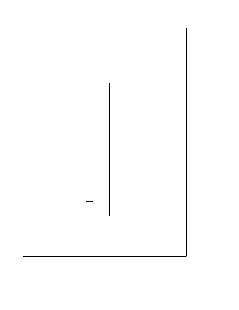
A memory map is shown inFigure 2 and register addressing
in Table III. They show the name, address and page loca-
tions for the LV8572A.
TABLE III. Register/Counter/RAM
Addressing for LV8572A
A0-4
PS
RS
Description
(Note 1) (Note 2)
CONTROL REGISTERS
00
03
04
01
02
03
04
X
0
0
0
0
0
0
X
0
0
1
1
1
1
Main Status Register
Periodic Flag Register
Time Save Control Register
Real Time Mode Register
Output Mode Register
Interrupt Control Register 0
Interrupt Control Register 1
COUNTERS (CLOCK CALENDAR)
05
06
07
08
09
0
0
0
0
0
X
X
X
X
X
1/100, 1/10 Seconds (0–99)
Seconds
Minutes
Hours
Days of
Month
Months
Years
Julian Date (LSB)
Julian Date
Day of Week
(0–59)
(0–59)
(1–12, 0–23)
(1–28/29/30/31)
(1–12)
(0–99)
(1–99)
(0–3)
(1–7)
0A
0B
0C
0D
0E
0
0
0
0
0
X
X
X
X
X
TIME COMPARE RAM
13
14
15
0
0
0
X
X
X
Sec Compare RAM
Min Compare RAM
Hours Compare
RAM
DOM Compare
RAM
Months Compare
RAM
DOW Compare RAM (1–7)
(0–59)
(0–59)
(1–12, 0–23)
16
0
X
(1–28/29/30/31)
17
0
X
(1–12)
18
0
X
TIME SAVE RAM
19
1A
1B
1C
1D
0
0
0
0
0
X
X
X
X
X
Seconds Time Save RAM
Minutes Time Save RAM
Hours Time Save RAM
Day of Month Time Save RAM
Months Time Save RAM
1E
1F
0
0
1
X
RAM
RAM/Test Mode Register
01–1F
1
X
2nd Page General Purpose RAM
1 PSDPage Select (Bit D7 of Main Status Register)
2 RSDRegister Select (Bit D6 of Main Status Register)
12
相關(guān)PDF資料 |
PDF描述 |
|---|---|
| LV8572AM | LV8572A Low Voltage Real Time Clock (RTC) |
| LV8572AN | LV8572A Low Voltage Real Time Clock (RTC) |
| LV8573A | LV8573A Low Voltage Real Time Clock (RTC) |
| LV8573AM | LV8573A Low Voltage Real Time Clock (RTC) |
| LV8573AN | LV8573A Low Voltage Real Time Clock (RTC) |
相關(guān)代理商/技術(shù)參數(shù) |
參數(shù)描述 |
|---|---|
| LV8572AM | 制造商:NSC 制造商全稱:National Semiconductor 功能描述:LV8572A Low Voltage Real Time Clock (RTC) |
| LV8572AMX | 制造商:未知廠家 制造商全稱:未知廠家 功能描述:Real-Time Clock |
| LV8572AN | 制造商:Rochester Electronics LLC 功能描述:- Bulk |
| LV8572AVX | 制造商:未知廠家 制造商全稱:未知廠家 功能描述:Real-Time Clock |
| LV8573A | 制造商:NSC 制造商全稱:National Semiconductor 功能描述:LV8573A Low Voltage Real Time Clock (RTC) |
發(fā)布緊急采購,3分鐘左右您將得到回復(fù)。