- 您現(xiàn)在的位置:買賣IC網(wǎng) > PDF目錄369873 > LV8571A PDF資料下載
參數(shù)資料
| 型號: | LV8571A |
| 文件頁數(shù): | 17/24頁 |
| 文件大小: | 353K |
| 代理商: | LV8571A |

Functional Description
(Continued)
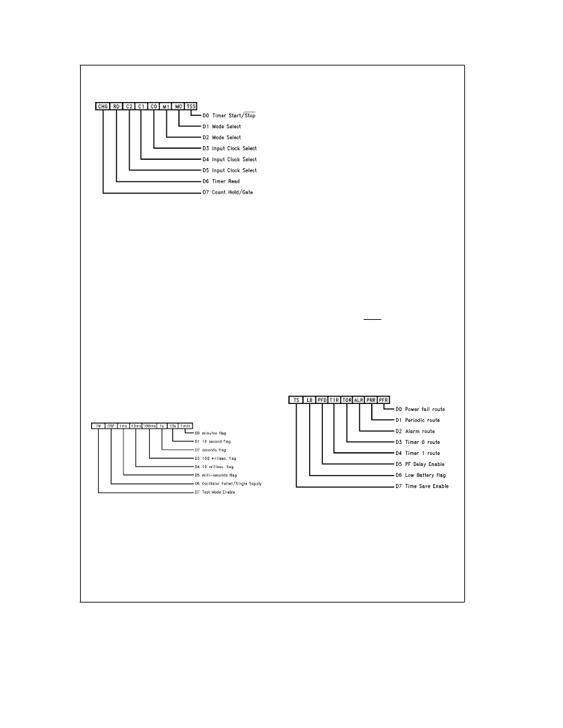
TIMER 0 AND 1 CONTROL REGISTER
TL/F/11416–17
These registers control the operation of the timers. Each
timer has its own register.
D0:
This bit will Start (1) or Stop (0) the timer. When the
timer is stopped the timer’s prescaler and counter are reset,
and the timer will restart from the beginning when started
again. In mode 0 on time out the TSS bit is internally reset.
D1 and D2:
These control the count mode of the timers.
See Table VI.
D3–D5:
These bits control which clock signal is applied to
the timer’s counter input. Refer to Table IV for details.
D6:
This is the read bit. If a one is written into this location it
will cause the contents of the timer to be latched into a
holding register, which can be read by the
m
P at any time.
Reading the least significant byte of the timer will reset the
RD bit. The timer read cycle can be aborted by writing RD to
zero.
D7:
The CHG bit has two mode dependent functions. In
modes 0 through 2 writing a one to this bit will suspend the
timer operation (without resetting the timer prescaler). How-
ever, in mode 3 this bit is used to trigger or re-trigger the
count sequence as with the gate pins. If retriggering is de-
sired using the CHG bit, it is not necessary to write a zero to
this location prior to the re-trigger. The action of further writ-
ing a one to this bit will re-trigger the count.
PERIODIC FLAG REGISTER
TL/F/11416–18
The Periodic Flag Register has the same bit for bit corre-
spondence as Interrupt Control Register 0 except for D6
and D7. For normal operation (i.e., not a single supply appli-
cation) this register must be written to on initial power up or
after an oscillator fail event. D0–D5 are read only bits, D6
and D7 are read/write.
D0–D5:
These bits are set by the real time rollover events:
(Time Change
e
1). The bits are reset when the register is
read and can be used as selective data change flags.
D6:
This bit performs a dual function. When this bit is read, a
one indicates that an oscillator failure has occurred and the
time information may have been lost. Some of the ways an
oscillator failure might be caused are: failure of the crystal,
shorting OSC IN or OSC OUT to GND or V
CC
, removal of
crystal, removal of battery when in the battery backed mode
(when a ‘‘0’’ is written to D6), lowering the voltage at the
V
BB
pin to a value less than 2.2V when in the battery
backed mode. Bit D6 is automatically set to 1 on initial pow-
er-up or an oscillator fail event. The oscillator fail flag is
reset by writing a one to the clock start/stop bit in the Real
Time Mode Register, with the crystal oscillating.
When D6 is written to, it defines whether the TCP is being
used in battery backed (normal) or in a single supply mode
application. When set to a one this bit configures the TCP
for single power supply applications. This bit is automatically
set on initial power-up or an oscillator fail event. When set,
D6 disables the oscillator reference circuit. The result is that
the oscillator is referenced to V
CC
. When a zero is written to
D6 the oscillator reference is enabled, thus the oscillator is
referenced to V
BB
. This allows operation in standard battery
standby applications.
At initial power on, if the LV8571A is going to be pro-
grammed for battery backed mode, the V
BB
pin should be
connected to a potential in the range of 2.2V to V
CC
-0.4V.
For single supply mode operation, the V
BB
pin should be
connected to GND and the PFAIL pin connected to V
CC
.
D7:
Writing a one to this bit enables the test mode register
at location 1F (see Table VII). This bit should be forced to
zero during initialization for normal operation. If the test
mode has been entered, clear the test mode register before
leaving test mode. (See separate test mode application
note for further details.)
INTERRUPT ROUTING REGISTER
TL/F/11416–19
D0–D4:
The lower 5 bits of this register are associated with
the main interrupt sources created by this chip. The purpose
of this register is to route the interrupts to either the MFO
(multi-function pin), or to the main interrupt pin. When any
bit is set the associated interrupt signal will be sent to the
MFO pin, and when zero it will be sent to the INTR pin.
17
相關(guān)PDF資料 |
PDF描述 |
|---|---|
| LV8572AMX | Real-Time Clock |
| LV8572AVX | Real-Time Clock |
| LV8800C | Optoelectronic |
| LVA12D | Analog IC |
| LVA12S | Analog IC |
相關(guān)代理商/技術(shù)參數(shù) |
參數(shù)描述 |
|---|---|
| LV8571AN | 制造商:Rochester Electronics LLC 功能描述:- Bulk 制造商:Texas Instruments 功能描述: |
| LV8572A | 制造商:NSC 制造商全稱:National Semiconductor 功能描述:LV8572A Low Voltage Real Time Clock (RTC) |
| LV8572AM | 制造商:NSC 制造商全稱:National Semiconductor 功能描述:LV8572A Low Voltage Real Time Clock (RTC) |
| LV8572AMX | 制造商:未知廠家 制造商全稱:未知廠家 功能描述:Real-Time Clock |
| LV8572AN | 制造商:Rochester Electronics LLC 功能描述:- Bulk |
發(fā)布緊急采購,3分鐘左右您將得到回復(fù)。