- 您現(xiàn)在的位置:買賣IC網(wǎng) > PDF目錄69008 > LTC6405CMS8E#PBF (LINEAR TECHNOLOGY CORP) SPECIALTY ANALOG CIRCUIT, PDSO8 PDF資料下載
參數(shù)資料
| 型號: | LTC6405CMS8E#PBF |
| 廠商: | LINEAR TECHNOLOGY CORP |
| 元件分類: | 模擬信號調(diào)理 |
| 英文描述: | SPECIALTY ANALOG CIRCUIT, PDSO8 |
| 封裝: | LEAD FREE, PLASTIC, MSOP-8 |
| 文件頁數(shù): | 13/24頁 |
| 文件大小: | 281K |
| 代理商: | LTC6405CMS8E#PBF |

LTC6405
20
6405fa
APPLICATIONS INFORMATION
The LTC6405’s input referred voltage noise contributes the
equivalent noise of a 155Ω resistor. When the feedback
network is comprised of resistors whose values are less
than this, the LTC6405’s output noise is voltage noise
dominant (see Figure 11):
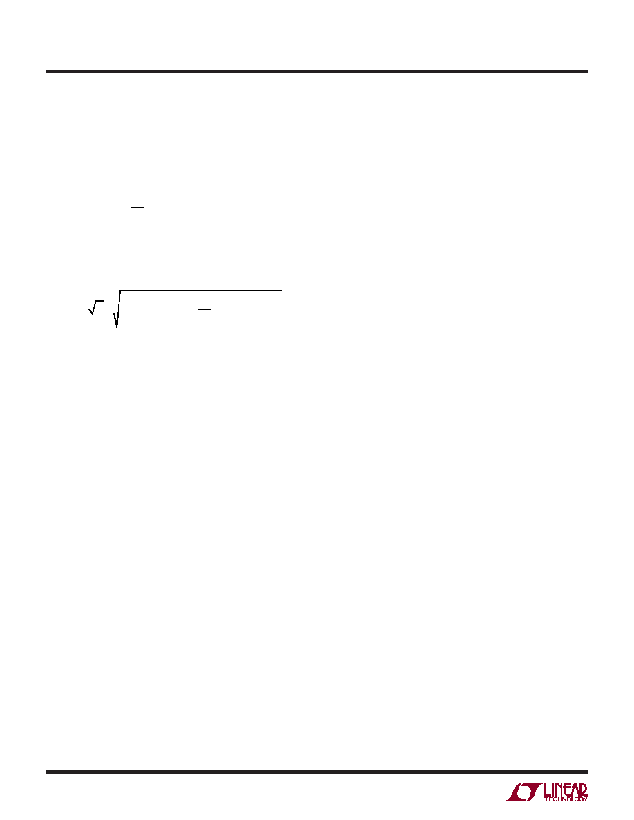
e
no ≈ eni 1+
R
F
R
I
Feedback networks consisting of resistors with values
greater than about 200Ω will result in output noise which
is resistor noise and amplier current noise dominant.
e
no ≈
2 I
n RF
()2 + 1+
R
F
R
I
4 k T R
F
Lower resistor values (<100Ω) always result in lower noise
at the penalty of increased distortion due to increased load-
ing of the feedback network on the output. Higher resistor
values (but still less than <500Ω) will result in higher
output noise, but typically improved distortion due to less
loading on the output. The optimal feedback resistance for
the LTC6405 runs in between 100Ω to 500Ω.
The differential ltered outputs +OUTF and –OUTF will
have a little higher noise than the unltered outputs (due
to the two 50Ω resistors which contribute 0.9nV/√Hz
each), but can provide superior signal-to-noise due to the
output noise ltering.
Layout Considerations
Because the LTC6405 is a very high speed amplier, it is
sensitive to both stray capacitance and stray inductance.
In the QFN package, three pairs of power supply pins are
provided to keep the power supply inductance as low
as possible to prevent any degradation of amplier 2nd
harmonic performance. It is critical that close attention be
paid to supply bypassing. For single supply applications
it is recommended that high quality 0.1μF surface mount
ceramic bypass capacitor be placed directly between each
V+ and V– pin with direct short connections. The V– pins
should be tied directly to a low impedance ground plane
with minimal routing. For dual (split) power supplies, it is
recommended that additional high quality, 0.1μF ceramic
capacitors are used to bypass V+ to ground and V– to
ground, again with minimal routing. For driving large loads
(<200Ω), additional bypass capacitance may be needed for
optimal performance. Keep in mind that small geometry
(e.g., 0603) surface mount ceramic capacitors have a much
higher self resonant frequency than do leaded capacitors,
and perform best in high speed applications.
Any stray parasitic capacitances to ground at the summing
junctions, +IN and –IN, should be minimized. This becomes
especially true when the feedback resistor network uses
resistor values >500Ω in circuits with RF = RI. Always keep
in mind the differential nature of the LTC6405, and that it
is critical that the load impedances seen by both outputs
(stray or intended), should be as balanced and symmetric
as possible. This will help preserve the natural balance
of the LTC6405, which minimizes the generation of even
order harmonics, and improves the rejection of common
mode signals and noise.
It is highly recommended that the VOCM pin be bypassed
to ground with a high quality ceramic capacitor whose
value exceeds 0.01μF. This will help stabilize the common
mode feedback loop as well as prevent thermal noise from
the internal voltage divider and other external sources of
noise from being converted to differential noise due to
divider mismatches in the feedback networks. It is also
recommended that the resistive feedback networks be
comprised of 1% resistors (or better) to enhance the
output common mode rejection. This will also prevent
VOCM input referred common mode noise of the common
mode amplier path (which cannot be ltered) from being
converted to differential noise, degrading the differential
noise performance.
Feedback factor mismatch has a weak effect on distortion.
Using 1% or better resistors will limit any mismatch from
impacting amplier linearity. However, in single supply
level shifting applications where there is a voltage differ-
ence between the input common mode voltage and the
output common mode voltage, resistor mismatch can
make the apparent voltage offset of the amplier appear
worse than specied.
相關(guān)PDF資料 |
PDF描述 |
|---|---|
| LTC693CS#TRPBF | 1-CHANNEL POWER SUPPLY SUPPORT CKT, PDSO16 |
| LTC692CN8#TRPBF | 1-CHANNEL POWER SUPPLY SUPPORT CKT, PDIP8 |
| LTM4600HVIV#TRPBF | 17 A SWITCHING REGULATOR, BGA104 |
| LTM4600HVEV#TRPBF | 17 A SWITCHING REGULATOR, BGA104 |
| LV5682P | 1-CHANNEL POWER SUPPLY SUPPORT CKT, ZFM25 |
相關(guān)代理商/技術(shù)參數(shù) |
參數(shù)描述 |
|---|---|
| LTC6405CMS8E-TRPBF | 制造商:LINER 制造商全稱:Linear Technology 功能描述:2.7GHz, 5V, Low Noise, Rail-to-Rail Input Differential Amplifi er/Driver |
| LTC6405CUD | 制造商:Linear Technology 功能描述:DIFF AMP 5V 2.7GHZ R/R 16QFN 制造商:Linear Technology 功能描述:DIFF AMP, 5V, 2.7GHZ, R/R, 16QFN |
| LTC6405CUD#PBF | 功能描述:IC DIFF AMP/DRIVER R-R 16-QFN RoHS:是 類別:集成電路 (IC) >> 線性 - 放大器 - 專用 系列:- 產(chǎn)品培訓(xùn)模塊:Lead (SnPb) Finish for COTS Obsolescence Mitigation Program 標準包裝:60 系列:- 類型:可變增益放大器 應(yīng)用:CATV 安裝類型:表面貼裝 封裝/外殼:20-WQFN 裸露焊盤 供應(yīng)商設(shè)備封裝:20-TQFN-EP(5x5) 包裝:托盤 |
| LTC6405CUD#TR | 制造商:Linear Technology 功能描述:DIFF-AMPLIFIER, 2.7GHZ, 690V/US, QFN-16, No. of Amplifiers:1, Input Offset Voltage:6mV, Bandwidth:2.7GHz, Amplifier Case Style:QFN, No. of Pins:16, Supply Voltage Range:4.5V to 5.25V, Slew Rate:690V/s, Supply Current:18mA, MSL:- , RoHS Compliant: No |
| LTC6405CUD#TRPBF | 功能描述:IC DIFF AMP/DRIVER R-R 16-QFN RoHS:是 類別:集成電路 (IC) >> 線性 - 放大器 - 專用 系列:- 產(chǎn)品培訓(xùn)模塊:Lead (SnPb) Finish for COTS Obsolescence Mitigation Program 標準包裝:60 系列:- 類型:可變增益放大器 應(yīng)用:CATV 安裝類型:表面貼裝 封裝/外殼:20-WQFN 裸露焊盤 供應(yīng)商設(shè)備封裝:20-TQFN-EP(5x5) 包裝:托盤 |
發(fā)布緊急采購,3分鐘左右您將得到回復(fù)。