- 您現(xiàn)在的位置:買賣IC網(wǎng) > PDF目錄377773 > LTC3204 (Linear Technology Corporation) Low Noise Regulated Charge Pump in 2 X 2 DFN PDF資料下載
參數(shù)資料
| 型號: | LTC3204 |
| 廠商: | Linear Technology Corporation |
| 英文描述: | Low Noise Regulated Charge Pump in 2 X 2 DFN |
| 中文描述: | 低噪聲電荷泵的2 × 2 DFN封裝 |
| 文件頁數(shù): | 8/12頁 |
| 文件大小: | 604K |
| 代理商: | LTC3204 |
LTC3204-3.3/LTC3204-5/
LTC3204B-3.3/LTC3204B-5
8
3204fa
Power Efficiency
The power efficiency (
η
) of the LTC3204-3.3/LTC3204-5/
LTC3204B-3.3/LTC3204B-5 is similar to that of a linear
regulator with an effective input voltage of twice the actual
input voltage. This occurs because the input current for a
voltage doubling charge pump is approximately twice the
output current. In an ideal regulating voltage doubler the
power efficiency would be given by:
IN
IN
OUT
At moderate to high output power, the switching losses
and the quiescent current of the LTC3204-3.3/LTC3204-5/
LTC3204B-3.3/LTC3204B-5 are negligible and the expres-
sion above is valid. For example, with V
IN
= 3V, I
OUT
=
100mA and V
OUT
regulating to 5V, the measured efficiency
is 81.8% which is in close agreement with the theoretical
83.3% calculation.
η =
=
=
P
P
V
V
I
I
V
2
V
OUT
OUT
OUT
OUT
IN
2
Maximum Available Output Current
For the LTC3204-3.3/LTC3204-5/LTC3204B-3.3/
LTC3204B-5,the maximum available output current and
voltage can be calculated from the effective open-loop
output resistance, R
OL
, and the effective input voltage,
2V
IN(MIN)
.
R
OL
(f
OSC
), value of the flying capacitor (C
FLY
), the nonoverlap
time, the internal switch resistances (R
S
), and the ESR of
the external capacitors. A first order approximation for
R
OL
is given below:
1
S=1 TO 4
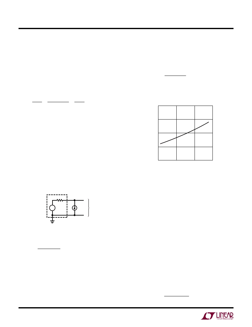
Typical R
OL
values as a function of temperature are shown
in Figure 2.
R
R
f
C
OL
S
OSC
FLY
∑
+
Figure 1. Equivalent Open-Loop Circuit
From Fig. 1, the available current is given by:
OL
I
V
V
R
OUT
IN
OUT
=
2
–
Effective Open Loop Output Resistance (R
OL
)
The effective open loop output resistance (R
OL
) of a charge
pump is a very important parameter which determines the
strength of the charge pump. The value of this parameter
depends on many factors such as the oscillator frequency
Figure 2. Typical R
OL
vs Temperature
V
IN
, V
OUT
Capacitor Selection
The style and value of capacitors used with the LTC3204-3.3/
LTC3204-5/LTC3204B-3.3/LTC3204B-5 determine several
important parameters such as regulator control loop sta-
bility, output ripple, charge pump strength and minimum
start-up time.
To reduce noise and ripple, it is recommended that low
ESR (<0.1
Ω
) ceramic capacitors be used for both C
IN
and
C
OUT
. These capacitors should be 1μF or greater. Tantalum
and aluminum capacitors are not recommended because
of their high ESR.
The value of C
OUT
directly controls the amount of output
ripple for a given load current. Increasing the size of C
OUT
will reduce the output ripple at the expense of higher
minimum turn-on time. The peak-to-peak output ripple
is approximately given by the expression:
OSC
OUT
V
I
f
C
RIPPLE P P
OUT
(
)
2
+
I
OUT
V
OUT
2V
IN
3204 F01
+
–
APPLICATIU
W
U
U
3204 F02
TEMPERATURE (
°
C)
100
0
50
E
)
V
IN
= 2.7V
V
OUT
= 4.5V
–50
8
7
6
5
4
相關PDF資料 |
PDF描述 |
|---|---|
| LTC3204BEDC-3.3 | Low Noise Regulated Charge Pump in 2 X 2 DFN |
| LTC3204BEDC-5 | Low Noise Regulated Charge Pump in 2 X 2 DFN |
| LTC3204-5 | Low Noise Regulated Charge Pump in 2 X 2 DFN |
| LTC3204B-3.3 | Low Noise Regulated Charge Pump in 2 X 2 DFN |
| LTC3204B-5 | Low Noise Regulated Charge Pump in 2 X 2 DFN |
相關代理商/技術參數(shù) |
參數(shù)描述 |
|---|---|
| LTC3204-3.3 | 制造商:LINER 制造商全稱:Linear Technology 功能描述:Low Noise Regulated Charge Pump in 2 X 2 DFN |
| LTC3204-5 | 制造商:LINER 制造商全稱:Linear Technology 功能描述:Low Noise Regulated Charge Pump in 2 X 2 DFN |
| LTC3204B-3.3 | 制造商:LINER 制造商全稱:Linear Technology 功能描述:Low Noise Regulated Charge Pump in 2 X 2 DFN |
| LTC3204B-5 | 制造商:LINER 制造商全稱:Linear Technology 功能描述:Low Noise Regulated Charge Pump in 2 X 2 DFN |
| LTC3204BEDC-3.3 | 制造商:LINER 制造商全稱:Linear Technology 功能描述:Low Noise Regulated Charge Pump in 2 X 2 DFN |
發(fā)布緊急采購,3分鐘左右您將得到回復。