- 您現(xiàn)在的位置:買賣IC網(wǎng) > PDF目錄377769 > LTC2404CG (LINEAR TECHNOLOGY CORP) 4-/8-Channel 24-Bit uPower No Latency ADCs PDF資料下載
參數(shù)資料
| 型號(hào): | LTC2404CG |
| 廠商: | LINEAR TECHNOLOGY CORP |
| 元件分類: | ADC |
| 英文描述: | 4-/8-Channel 24-Bit uPower No Latency ADCs |
| 中文描述: | 4-CH 24-BIT DELTA-SIGMA ADC, SERIAL ACCESS, PDSO28 |
| 封裝: | 0.209 INCH, PLASTIC, SSOP-28 |
| 文件頁數(shù): | 23/36頁 |
| 文件大小: | 351K |
| 代理商: | LTC2404CG |
第1頁第2頁第3頁第4頁第5頁第6頁第7頁第8頁第9頁第10頁第11頁第12頁第13頁第14頁第15頁第16頁第17頁第18頁第19頁第20頁第21頁第22頁當(dāng)前第23頁第24頁第25頁第26頁第27頁第28頁第29頁第30頁第31頁第32頁第33頁第34頁第35頁第36頁
23
LTC2404/LTC2408
APPLICATIO
S I
N
FOR
ATIO
U
power dissipation. A series resistor between 27
and 56
placed near the driver or near the LTC2404/LTC2408 pin
will also eliminate this problem without additional power
dissipation. The actual resistor value depends upon the
trace impedance and connection topology.
W
U
Driving the Input and Reference
The analog input and reference of the typical delta-sigma
analog-to-digital converter are applied to a switched ca-
pacitor network. This network consists of capacitors switch-
ing between the analog input (ADCIN), COM (Pin 6) and
the reference (V
REF
). The result is small current spikes
seen at both ADCIN and V
REF
. A simplified input equivalent
circuit is shown in Figure 12.
The key to understanding the effects of this dynamic input
current is based on a simple first order RC time constant
model. Using the internal oscillator, the internal switched
capacitor network of the LTC2404/LTC2408 is clocked at
153,600Hz corresponding to a 6.5
μ
s sampling period.
Fourteen time constants are required each time a capacitor
is switched in order to achieve 1ppm settling accuracy.
Therefore, the equivalent time constant at V
IN
and V
REF
should be less than 6.5
μ
s/14 = 460ns in order to achieve
1ppm accuracy.
Input Current (V
IN
)
If complete settling occurs on the input, conversion re-
sults will be uneffected by the dynamic input current. If the
settling is incomplete, it does not degrade the linearity
performance of the device. It simply results in an offset/
full-scale shift, see Figure 13. To simplify the analysis of
input dynamic current, two separate cases are assumed:
large capacitance at V
IN
(C
IN
> 0.01
μ
F) and small capaci-
tance at V
IN
(C
IN
< 0.01
μ
F).
If the total capacitance at V
IN
(see Figure 14) is small
(<0.01
μ
F), relatively large external source resistances (up
to 20k for 20pF parasitic capacitance) can be tolerated
without any offset/full-scale error. Figures 15 and 16 show
a family of offset and full-scale error curves for various
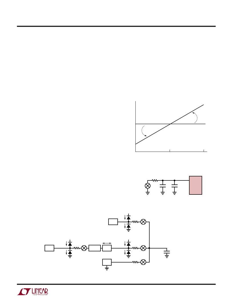
Figure 12. LTC2404/LTC2408 Equivalent Analog Input Circuit
V
REF
CHX
ADCV
CC
(PIN 2)
R
SW
5k
AVERAGE INPUT CURRENT:
I
DC
= 0.25(V
IN
– 0.5 V
REF
) f C
EQ
I
REF
I
REF
ADCV
CC
(PIN 2)
I
IN(LEAK)
I
IN(LEAK)
±
I
DC
MUXV
CC
(PIN 8)
I
IN(MUX)
I
IN(MUX)
R
SW
5k
R
SW
75
C
EQ
10pF (TYP)
R
SW
5k
SELECTED
CHANNEL
24048 F12
f
OUT
= 50Hz, INTERNAL OSCILLATOR: f = 128kHz
f
= 60Hz, INTERNAL OSCILLATOR: f = 153.6kHz
EXTERNAL OSCILLATOR: 2.56kHz
≤
f
≤
307.2kHz
COM
ADCIN
MUXOUT
Figure 13. Offset/Full-Scale Shift
Figure 14. An RC Network at CH0 to CH7
C
IN
24048 F14
INTPUT
SIGNAL
SOURCE
R
SOURCE
CH0 TO
CH7
LTC2404/
LTC2408
C
PAR
0
TUE
V
REF
/2
V
IN
24048 F13
V
REF
發(fā)布緊急采購,3分鐘左右您將得到回復(fù)。