- 您現(xiàn)在的位置:買賣IC網(wǎng) > PDF目錄39416 > LTC2285IUP#3CGPBF (LINEAR TECHNOLOGY CORP) PROPRIETARY METHOD ADC, PQCC64 PDF資料下載
參數(shù)資料
| 型號: | LTC2285IUP#3CGPBF |
| 廠商: | LINEAR TECHNOLOGY CORP |
| 元件分類: | ADC |
| 英文描述: | PROPRIETARY METHOD ADC, PQCC64 |
| 封裝: | 9 X 9 MM, LEAD FREE, PLASTIC, QFN-64 |
| 文件頁數(shù): | 9/24頁 |
| 文件大?。?/td> | 578K |
| 代理商: | LTC2285IUP#3CGPBF |
LTC2285IUP#3CGPBF
17
2285iup#3cgpbf
APPLICATIONS INFORMATION
storing analog signals on small valued capacitors. Junction
leakage will discharge the capacitors. The specied mini-
mum operating frequency for the LTC2285IUP#3CGPBF
is 1Msps.
Clock Duty Cycle Stabilizer
An optional clock duty cycle stabilizer circuit ensures
high performance even if the input clock has a non
50% duty cycle. Using the clock duty cycle stabilizer is
recommended for most applications. To use the clock
duty cycle stabilizer, the MODE pin should be connected
to 1/3VDD or 2/3VDD using external resistors.
This circuit uses the rising edge of the CLK pin to sample
the analog input. The falling edge of CLK is ignored and
the internal falling edge is generated by a phase-locked
loop. The input clock duty cycle can vary from 40% to 60%
and the clock duty cycle stabilizer will maintain a constant
50% internal duty cycle. If the clock is turned off for a
long period of time, the duty cycle stabilizer circuit will
require a hundred clock cycles for the PLL to lock onto the
input clock.
For applications where the sample rate needs to be changed
quickly, the clock duty cycle stabilizer can be disabled. If
the duty cycle stabilizer is disabled, care should be taken to
make the sampling clock have a 50% (±5%) duty cycle.
DIGITAL OUTPUTS
Table 1 shows the relationship between the analog input
voltage, the digital data bits, and the overow bit. Note that
OF is high when an overow or underow has occurred
on either channel A or channel B.
Table 1. Output Codes vs Input Voltage
AIN+ – AIN–
(2V Range)
OF
D13 – D0
(Offset Binary)
D13 – D0
(2’s Complement)
>+1.000000V
+0.999878V
+0.999756V
1
0
11 1111 1111 1111
11 1111 1111 1110
01 1111 1111 1111
01 1111 1111 1110
+0.000122V
0.000000V
–0.000122V
–0.000244V
0
10 0000 0000 0001
10 0000 0000 0000
01 1111 1111 1111
01 1111 1111 1110
00 0000 0000 0001
00 0000 0000 0000
11 1111 1111 1111
11 1111 1111 1110
–0.999878V
–1.000000V
<–1.000000V
0
1
00 0000 0000 0001
00 0000 0000 0000
10 0000 0000 0001
10 0000 0000 0000
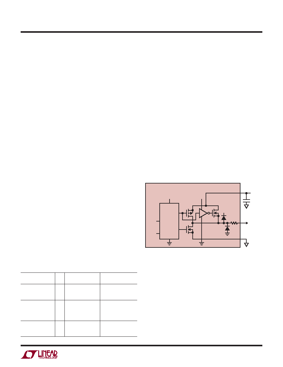
Digital Output Buffers
Figure 14 shows an equivalent circuit for a single out-
put buffer. Each buffer is powered by OVDD and OGND,
isolated from the ADC power and ground. The additional
N-channel transistor in the output driver allows operation
down to low voltages. The internal resistor in series with
the output makes the output appear as 50Ω to external
circuitry and may eliminate the need for external damping
resistors.
As with all high speed/high resolution converters, the
digital output loading can affect the performance. The
digital outputs of the LTC2285IUP#3CGPBF should drive
a minimal capacitive load to avoid possible interaction
between the digital outputs and sensitive input circuitry.
For full speed operation the capacitive load should be
kept under 10pF.
Lower OVDD voltages will also help reduce interference
from the digital outputs.
Figure 14. Digital Output Buffer
LTC2285IUP#3CGPBF
2285 F14
OVDD
VDD
0.1μF
43Ω
TYPICAL
DATA
OUTPUT
OGND
OVDD
0.5V
TO 3.6V
PREDRIVER
LOGIC
DATA
FROM
LATCH
OE
Data Format
Using the MODE pin, the LTC2285IUP#3CGPBF parallel
digital output can be selected for offset binary or 2’s
complement format. Connecting MODE to GND or 1/3VDD
selects offset binary output format. Connecting MODE to
2/3VDD or VDD selects 2’s complement output format. An
external resistor divider can be used to set the 1/3VDD or
2/3VDD logic values. Table 2 shows the logic states for
the MODE pin.
相關(guān)PDF資料 |
PDF描述 |
|---|---|
| LTC2305CDE#PBF | 2-CH 12-BIT SUCCESSIVE APPROXIMATION ADC, SERIAL ACCESS, PDSO12 |
| LTC2305CMS#PBF | 2-CH 12-BIT SUCCESSIVE APPROXIMATION ADC, SERIAL ACCESS, PDSO12 |
| LTC2305IDE#PBF | 2-CH 12-BIT SUCCESSIVE APPROXIMATION ADC, SERIAL ACCESS, PDSO12 |
| LTC2305IDE#TRPBF | 2-CH 12-BIT SUCCESSIVE APPROXIMATION ADC, SERIAL ACCESS, PDSO12 |
| LTC2305IMS#PBF | 2-CH 12-BIT SUCCESSIVE APPROXIMATION ADC, SERIAL ACCESS, PDSO12 |
相關(guān)代理商/技術(shù)參數(shù) |
參數(shù)描述 |
|---|---|
| LTC2285IUPPBF | 制造商:Linear Technology 功能描述:ADC, Dual 14b 125Msps, 3V, LTC2285IUP |
| LTC2285IUP-PBF | 制造商:LINER 制造商全稱:Linear Technology 功能描述:Dual 14-Bit, 125Msps Low Power 3V ADC |
| LTC2285IUP-TR | 制造商:LINER 制造商全稱:Linear Technology 功能描述:Dual 14-Bit, 125Msps Low Power 3V ADC |
| LTC2285IUP-TRPBF | 制造商:LINER 制造商全稱:Linear Technology 功能描述:Dual 14-Bit, 125Msps Low Power 3V ADC |
| LTC2285UP | 制造商:LINER 制造商全稱:Linear Technology 功能描述:Dual 14-Bit, 135Msps Low Power 3.3V ADC |
發(fā)布緊急采購,3分鐘左右您將得到回復(fù)。