- 您現(xiàn)在的位置:買賣IC網(wǎng) > PDF目錄296330 > LTC2207IUK#PBF (LINEAR TECHNOLOGY CORP) 16-Bit, 105Msps ADC; Package: QFN; No of Pins: 48; Temperature Range: -40°C to +85°C PDF資料下載
參數(shù)資料
第1頁第2頁第3頁第4頁第5頁第6頁第7頁第8頁第9頁第10頁第11頁第12頁第13頁第14頁第15頁第16頁第17頁第18頁第19頁第20頁第21頁第22頁當(dāng)前第23頁第24頁第25頁第26頁第27頁第28頁第29頁第30頁第31頁第32頁
LTC2207/LTC2206
3
22076fc
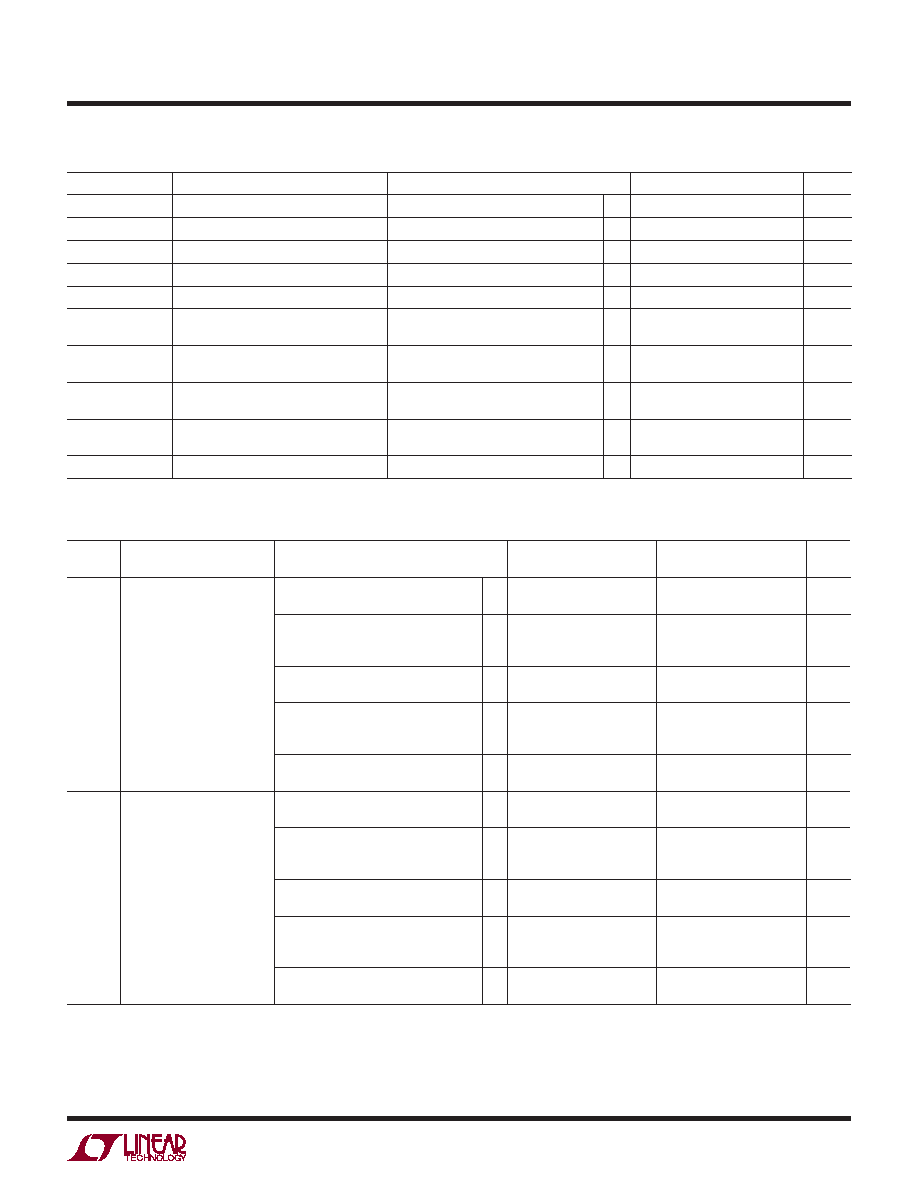
The ● denotes the specications which apply over the full operating temperature range, otherwise
specications are at TA = 25°C. (Note 4)
ANALOG INPUT
The ● denotes the specications which apply over the full operating temperature range,
otherwise specications are at TA = 25°C. AIN = –1dBFS. (Note 4)
SYMBOL PARAMETER
CONDITIONS
MIN
LTC2206
TYP
MAX
MIN
LTC2207
TYP
MAX
UNITS
SNR
Signal-to-Noise Ratio
5MHz Input (2.25V Range, PGA = 0)
5MHz Input (1.5V Range, PGA = 1)
77.9
75.5
77.9
75.5
dBFS
15MHz Input (2.25V Range, PGA = 0),
15MHz Input (2.25V Range, PGA = 0)
15MHz Input (1.5V Range, PGA = 1)
●
76.5
76.2
77.8
77.5
75.4
76.5
76.2
77.8
77.5
75.4
dBFS
70MHz Input (2.25V Range, PGA = 0)
70MHz Input (1.5V Range, PGA = 1)
77.5
75.3
77.5
75.3
dBFS
140MHz Input (2.25V Range, PGA = 0)
140MHz Input (1.5V Range, PGA = 1),
140MHz Input (1.5V Range, PGA = 1)
●
73.8
73.4
76.7
74.8
74.5
73.8
73.4
76.7
74.8
74.5
dBFS
170MHz Input (2.25V Range, PGA = 0)
170MHz Input (1.5V Range, PGA = 1)
76.2
75.4
76.2
75.4
dBFS
SFDR
Spurious Free
Dynamic Range
2nd or 3rd
Harmonic
5MHz Input (2.25V Range, PGA = 0)
5MHz Input (1.5V Range, PGA = 1)
100
dBc
15MHz Input (2.25V Range, PGA = 0),
15MHz Input (2.25V Range, PGA = 0)
15MHz Input (1.5V Range, PGA = 1)
●
87
86
95
100
88
87
95
100
dBc
70MHz Input (2.25V Range, PGA = 0)
70MHz Input (1.5V Range, PGA = 1)
90
95
90
95
dBc
140MHz Input (2.25V Range, PGA = 0)
140MHz Input (1.5V Range, PGA = 1),
140MHz Input (1.5V Range, PGA = 1)
●
84
83
85
90
89
84
83
85
90
89
dBc
170MHz Input (2.25V Range, PGA = 0)
170MHz Input (1.5V Range, PGA = 1)
82
86
82
86
dBc
DYNAMIC ACCURACY
SYMBOL
PARAMETER
CONDITIONS
MIN
TYP
MAX
UNITS
VIN
Analog Input Range (AIN+ – AIN–)
3.135V ≤ VDD ≤ 3.465V
●
1.5 to 2.25
VP-P
VIN, CM
Analog Input Common Mode
Differential Input (Note 7)
●
1
1.25
1.5
V
IIN
Analog Input Leakage Current
0V ≤ AIN+, AIN– ≤ VDD (Note 10)
●
1μA
ISENSE
SENSE Input Leakage Current
0V ≤ SENSE ≤ VDD (Note 11)
●
–3
3
μA
IMODE
MODE Pin Pull-Down Current to GND
10
μA
CIN
Analog Input Capacitance
Sample Mode ENC+ < ENC–
Hold Mode ENC+ > ENC–
6.7
1.8
pF
tAP
Sample-and-Hold
Acquisition Delay Time
1ns
tJITTER
Sample-and-Hold
Acquisition Delay Time Jitter
80
fsRMS
CMRR
Analog Input
Common Mode Rejection Ratio
1V < (AIN+ = AIN–) <1.5V
80
dB
BW-3dB
Full Power Bandwidth
RS ≤ 25Ω
700
MHz
相關(guān)PDF資料 |
PDF描述 |
|---|---|
| LTC2207IUK#TRPBF | 16-Bit, 105Msps ADC; Package: QFN; No of Pins: 48; Temperature Range: -40°C to +85°C |
| LTC2208CUP-14#PBF | 16-Bit, 130Msps ADC; Package: QFN; No of Pins: 64; Temperature Range: 0°C to +70°C |
| LTC2208CUP#PBF | 16-Bit, 130Msps ADC; Package: QFN; No of Pins: 64; Temperature Range: 0°C to +70°C |
| LTC2208CUP#TRPBF | 16-Bit, 130Msps ADC; Package: QFN; No of Pins: 64; Temperature Range: 0°C to +70°C |
| LTC2411CMS | Analog-to-Digital Converter, 24-Bit |
相關(guān)代理商/技術(shù)參數(shù) |
參數(shù)描述 |
|---|---|
| LTC2207UK | 制造商:LINER 制造商全稱:Linear Technology 功能描述:16-Bit, 105Msps/80Msps ADCs |
| LTC2207UK-14 | 制造商:LINER 制造商全稱:Linear Technology 功能描述:14-Bit, 105Msps/80Msps ADCs |
| LTC2208 | 制造商:LINER 制造商全稱:Linear Technology 功能描述:Dual 14-Bit 250Msps |
| LTC2208-14 | 制造商:LINER 制造商全稱:Linear Technology 功能描述:14-Bit, 130Msps ADC |
| LTC2208CUP | 制造商:Linear Technology 功能描述:IC ADC 16BIT 130MSPS 64-QFN |
發(fā)布緊急采購,3分鐘左右您將得到回復(fù)。