- 您現(xiàn)在的位置:買賣IC網(wǎng) > PDF目錄39412 > LTC2161IUK#TRPBF (LINEAR TECHNOLOGY CORP) 1-CH 16-BIT PROPRIETARY METHOD ADC, PARALLEL ACCESS, PQCC48 PDF資料下載
參數(shù)資料
| 型號(hào): | LTC2161IUK#TRPBF |
| 廠商: | LINEAR TECHNOLOGY CORP |
| 元件分類: | ADC |
| 英文描述: | 1-CH 16-BIT PROPRIETARY METHOD ADC, PARALLEL ACCESS, PQCC48 |
| 封裝: | 7 X 7 MM, LEAD FREE, PLASTIC, MO-220WKKD-2, QFN-48 |
| 文件頁數(shù): | 11/36頁 |
| 文件大小: | 651K |
| 代理商: | LTC2161IUK#TRPBF |
第1頁第2頁第3頁第4頁第5頁第6頁第7頁第8頁第9頁第10頁當(dāng)前第11頁第12頁第13頁第14頁第15頁第16頁第17頁第18頁第19頁第20頁第21頁第22頁第23頁第24頁第25頁第26頁第27頁第28頁第29頁第30頁第31頁第32頁第33頁第34頁第35頁第36頁
LTC2162/LTC2161/LTC2160
19
216210f
applicaTions inForMaTion
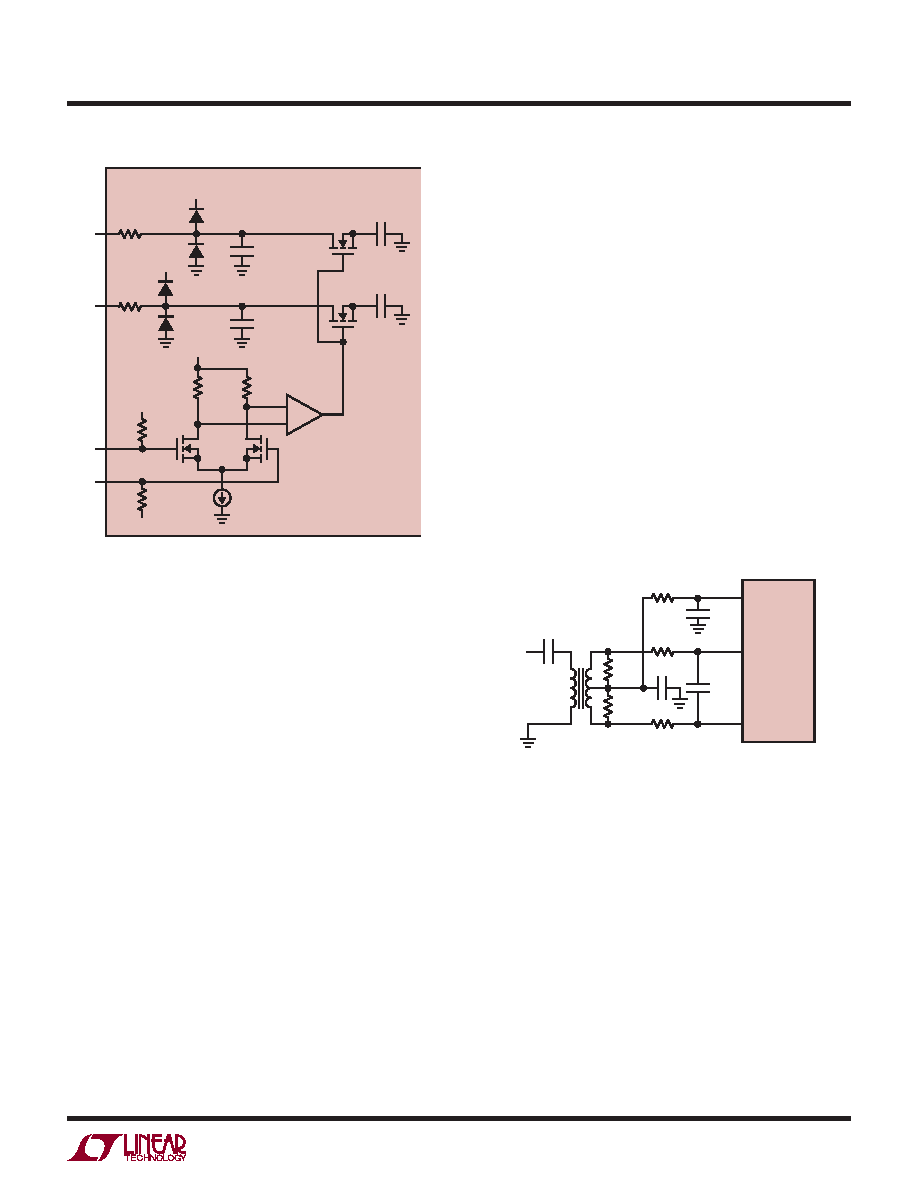
Figure 2. Equivalent Input Circuit
Transformer Coupled Circuits
Figure 3 shows the analog input being driven by an RF
transformer with a center-tapped secondary. The center
tap is biased with VCM, setting the A/D input at its optimal
DC level. At higher input frequencies a transmission line
balun transformer (Figures 4 through 6) has better bal-
ance, resulting in lower A/D distortion.
Amplifier Circuits
Figure 7 shows the analog input being driven by a high
speed differential amplifier. The output of the amplifier is
AC coupled to the A/D so the amplifier’s output common
mode voltage can be optimally set to minimize distortion.
At very high frequencies an RF gain block will often have
lower distortion than a differential amplifier. If the gain
block is single-ended, then a transformer circuit (Figures 4
through 6) should convert the signal to differential before
driving the A/D.
Figure 3. Analog Input Circuit Using a Transformer.
Recommended for Input Frequencies from 5MHz to 70MHz
CSAMPLE
5pF
RON
15
RON
15
VDD
LTC2162
AIN+
216210 F02
CSAMPLE
5pF
VDD
AIN–
ENC–
ENC+
1.2V
10k
1.2V
10k
CPARASITIC
1.8pF
CPARASITIC
1.8pF
10
25
50
AIN+
AIN–
12pF
0.1F
VCM
LTC2162
ANALOG
INPUT
0.1F
T1
1:1
T1: MA/COM MABAES0060 RESISTORS,
CAPACITORS ARE 0402 PACKAGE SIZE
216210 F03
0.1F
Single-Ended Input
For applications less sensitive to harmonic distortion, the
AIN+ input can be driven single-ended with a 1VP-P signal
centered around VCM. The AIN– input should be connected
to VCM and the VCM bypass capacitor should be increased
to 2.2F. With a single-ended input the harmonic distortion
and INL will degrade, but the noise and DNL will remain
unchanged.
INPUT DRIVE CIRCUITS
Input filtering
If possible, there should be an RC lowpass filter right at
the analog inputs. This lowpass filter isolates the drive
circuitryfromtheA/Dsample-and-holdswitching,andalso
limits wideband noise from the drive circuitry. Figure 3
shows an example of an input RC filter. The RC component
values should be chosen based on the application’s input
frequency.
相關(guān)PDF資料 |
PDF描述 |
|---|---|
| LTC2161CUK#PBF | 1-CH 16-BIT PROPRIETARY METHOD ADC, PARALLEL ACCESS, PQCC48 |
| LTC2164CUK#TRPBF | 1-CH 16-BIT PROPRIETARY METHOD ADC, PARALLEL ACCESS, PQCC48 |
| LTC2164IUK#PBF | 1-CH 16-BIT PROPRIETARY METHOD ADC, PARALLEL ACCESS, PQCC48 |
| LTC2163CUK#TRPBF | 1-CH 16-BIT PROPRIETARY METHOD ADC, PARALLEL ACCESS, PQCC48 |
| LTC2163IUK#TRPBF | 1-CH 16-BIT PROPRIETARY METHOD ADC, PARALLEL ACCESS, PQCC48 |
相關(guān)代理商/技術(shù)參數(shù) |
參數(shù)描述 |
|---|---|
| LTC2162 | 制造商:LINER 制造商全稱:Linear Technology 功能描述:Precision, Low Power Rail-to-Rail Input/Output |
| LTC2162-14 | 制造商:LINER 制造商全稱:Linear Technology 功能描述:High Linearity Differential RF/IF Amplifier/ADC Driver |
| LTC2162CUK#PBF | 制造商:Linear Technology 功能描述:ADC Single 65Msps 16-bit Parallel/Serial (SPI)/LVDS 48-Pin QFN EP 制造商:Linear Technology 功能描述:IC ADC 16BIT 65 MSPS 48-QFN 制造商:Linear Technology 功能描述:ADC 16BIT 65MSPS 48QFN 制造商:Linear Technology 功能描述:ADC, 16BIT, 65MSPS, 48QFN |
| LTC2162CUK#TRPBF | 制造商:Linear Technology 功能描述:ADC Single 65Msps 16-bit Parallel/Serial (SPI)/LVDS 48-Pin QFN EP T/R 制造商:Linear Technology 功能描述:IC ADC 16BIT 65 MSPS 48-QFN |
| LTC2162IUK#PBF | 制造商:Linear Technology 功能描述:ADC Single 65Msps 16-bit Parallel/Serial (SPI)/LVDS 48-Pin QFN EP 制造商:Linear Technology 功能描述:Single ADC 65Msps 16-bit Parallel/Serial (SPI)/LVDS 48-Pin QFN EP 制造商:Linear Technology 功能描述:IC ADC 16BIT 65 MSPS 48-QFN 制造商:Linear Technology 功能描述:MS-ADC/High Speed, 16-bit, 65Msps, 1.8V Low-Power ADC, Parallel Outputs |
發(fā)布緊急采購,3分鐘左右您將得到回復(fù)。