- 您現(xiàn)在的位置:買賣IC網(wǎng) > PDF目錄39411 > LTC2157CUP-14#PBF (LINEAR TECHNOLOGY CORP) 2-CH 14-BIT PROPRIETARY METHOD ADC, PARALLEL ACCESS, PQCC64 PDF資料下載
參數(shù)資料
| 型號: | LTC2157CUP-14#PBF |
| 廠商: | LINEAR TECHNOLOGY CORP |
| 元件分類: | ADC |
| 英文描述: | 2-CH 14-BIT PROPRIETARY METHOD ADC, PARALLEL ACCESS, PQCC64 |
| 封裝: | 9 X 9 MM, LEAD FREE, PLASTIC, MO-220WNJR-5, QFN-64 |
| 文件頁數(shù): | 6/32頁 |
| 文件大小: | 647K |
| 代理商: | LTC2157CUP-14#PBF |
第1頁第2頁第3頁第4頁第5頁當前第6頁第7頁第8頁第9頁第10頁第11頁第12頁第13頁第14頁第15頁第16頁第17頁第18頁第19頁第20頁第21頁第22頁第23頁第24頁第25頁第26頁第27頁第28頁第29頁第30頁第31頁第32頁
LTC2157-14/
LTC2156-14/LTC2155-14
14
21576514f
PIN FUNCTIONS
LVDS Outputs
The following pins are differential LVDS outputs. The
output current level is programmable. There is an optional
internal 100Ω termination resistor between the pins of
each LVDS output pair.
OF–/OF+ (Pins 22/23):
Over/Underflow Digital Output.
OF+ is high when an overflow or underflow has occurred.
The overflows for channel A and channel B are multiplexed
together.
DB0_1–/DB0_1+ to DB12_13–/DB12_13+ (Pins 24/25, 26/27,
28/29, 30/31, 34/35, 36/37, 38/39): Channel B Double
Data Rate Digital Outputs. Two data bits are multiplexed
onto each differential output pair. The even data bits (DB0,
DB2, DB4, DB6, DB8, DB10, DB12) appear when CLKOUT+
is low. The odd data bits (DB1, DB3, DB5, DB7, DB9, DB11,
DB13) appear when CLKOUT+ is high.
CLKOUT–/CLKOUT+ (Pins 40/41):
Data Output Clock.
The digital outputs normally transition at the same time
as the falling and rising edges of CLKOUT+. The phase of
CLKOUT+ can also be delayed relative to the digital outputs
by programming the mode control registers.
DA0_1–/DA0_1+ to DA12_13–/DA12_13+ (Pins 42/43, 44/45,
46/47, 50/51, 52/53, 54/55, 56/57): Channel A Double
Data Rate Digital Outputs. Two data bits are multiplexed
onto each differential output pair. The even data bits (DA0,
DA2, DA4, DA6, DA8, DA10, DA12) appear when CLKOUT+
is low. The odd data bits (DA1, DA3, DA5, DA7, DA9, DA11,
DA13) appear when CLKOUT+ is high.
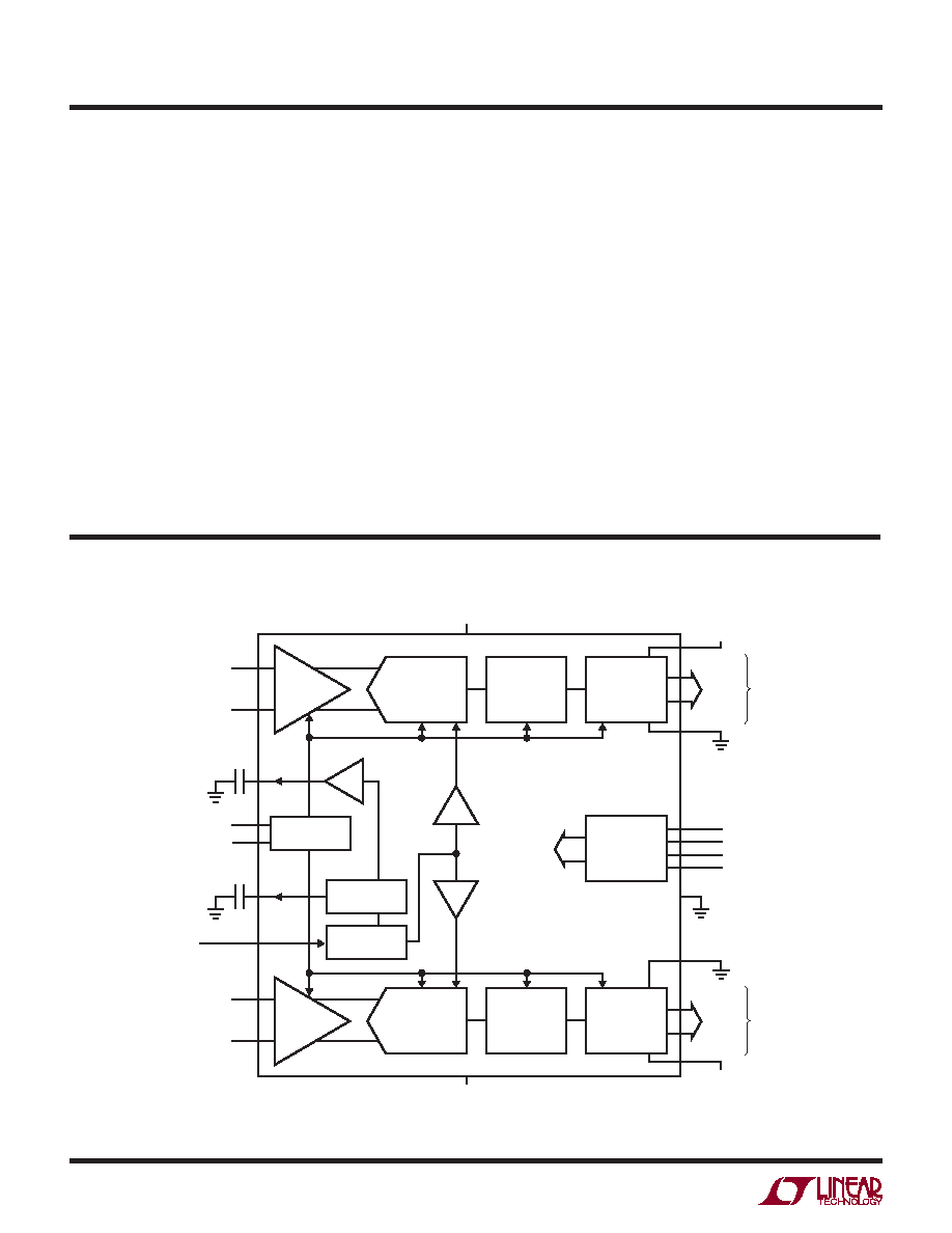
FUNCTIONAL BLOCK DIAGRAM
Figure 1. Functional Block Diagram
S/H
VCM
BUFFER
GND
VCM
0.1μF
CORRECTION
LOGIC
OUTPUT
DRIVERS
14-BIT
PIPELINED
ADC CORE
CLOCK/DUTY
CYCLE CONTROL
1.25V
REFERENCE
RANGE
SELECT
CLOCK
ANALOG
INPUT
21576514 F01
DDR
LVDS
DDR
LVDS
VDD
OVDD
OGND
CS
CHANNEL A
CHANNEL B
S/H
CORRECTION
LOGIC
OUTPUT
DRIVERS
SPI
14-BIT
PIPELINED
ADC CORE
ANALOG
INPUT
OVDD
OGND
VREF
2.2μF
GND
SENSE
SCK
SDI
PAR/SER
DA12_13
DA0_1
DB12_13
DB0_1
相關(guān)PDF資料 |
PDF描述 |
|---|---|
| LTC2157CUP-14#TRPBF | 2-CH 14-BIT PROPRIETARY METHOD ADC, PARALLEL ACCESS, PQCC64 |
| LTC2157IUP-14#PBF | 2-CH 14-BIT PROPRIETARY METHOD ADC, PARALLEL ACCESS, PQCC64 |
| LTC2155IUP-14#TRPBF | 2-CH 14-BIT PROPRIETARY METHOD ADC, PARALLEL ACCESS, PQCC64 |
| LTC2156IUP-14#PBF | 2-CH 14-BIT PROPRIETARY METHOD ADC, PARALLEL ACCESS, PQCC64 |
| LTC2155CUP-14#PBF | 2-CH 14-BIT PROPRIETARY METHOD ADC, PARALLEL ACCESS, PQCC64 |
相關(guān)代理商/技術(shù)參數(shù) |
參數(shù)描述 |
|---|---|
| LTC2157IUP-12#PBF | 制造商:Linear Technology 功能描述:ADC Dual Pipelined 250Msps 12-bit Parallel/Serial (SPI)/LVDS 64-Pin QFN EP 制造商:Linear Technology 功能描述:IC ADC DUAL 12BIT 250M 64-QFN |
| LTC2157IUP-12#TRPBF | 制造商:Linear Technology 功能描述:ADC Dual Pipelined 250Msps 12-bit Parallel/Serial (SPI)/LVDS 64-Pin QFN EP T/R 制造商:Linear Technology 功能描述:IC ADC DUAL 12BIT 250M 64-QFN |
| LTC2157IUP-14#PBF | 制造商:Linear Technology 功能描述:Dual ADC Pipelined 250Msps 14-bit Parallel/Serial (SPI)/LVDS 64-Pin QFN EP 制造商:Linear Technology 功能描述:IC ADC DUAL 250MSPS 64-QFN |
| LTC2157IUP-14#TRPBF | 制造商:Linear Technology 功能描述:IC ADC DUAL 250MSPS 64-QFN |
| LTC2158-14 | 制造商:LINER 制造商全稱:Linear Technology 功能描述:30MHz to 1.4GHz IQ Demodulator |
發(fā)布緊急采購,3分鐘左右您將得到回復。