- 您現(xiàn)在的位置:買(mǎi)賣(mài)IC網(wǎng) > PDF目錄30769 > LTC1871IMS-1#TR (LINEAR TECHNOLOGY CORP) SWITCHING CONTROLLER, 1000 kHz SWITCHING FREQ-MAX, PDSO10 PDF資料下載
參數(shù)資料
| 型號(hào): | LTC1871IMS-1#TR |
| 廠商: | LINEAR TECHNOLOGY CORP |
| 元件分類: | 穩(wěn)壓器 |
| 英文描述: | SWITCHING CONTROLLER, 1000 kHz SWITCHING FREQ-MAX, PDSO10 |
| 封裝: | PLASTIC, MSOP-10 |
| 文件頁(yè)數(shù): | 36/36頁(yè) |
| 文件大?。?/td> | 523K |
| 代理商: | LTC1871IMS-1#TR |
第1頁(yè)第2頁(yè)第3頁(yè)第4頁(yè)第5頁(yè)第6頁(yè)第7頁(yè)第8頁(yè)第9頁(yè)第10頁(yè)第11頁(yè)第12頁(yè)第13頁(yè)第14頁(yè)第15頁(yè)第16頁(yè)第17頁(yè)第18頁(yè)第19頁(yè)第20頁(yè)第21頁(yè)第22頁(yè)第23頁(yè)第24頁(yè)第25頁(yè)第26頁(yè)第27頁(yè)第28頁(yè)第29頁(yè)第30頁(yè)第31頁(yè)第32頁(yè)第33頁(yè)第34頁(yè)第35頁(yè)當(dāng)前第36頁(yè)

LTC1871-1
9
18711fb
OPERATION
MOSFET RDS(ON). If the ITH pin drops below 0.175V, the
Burst Mode comparator B1 will turn off the power MOSFET
and scale back the quiescent current of the IC to 250μA
(sleep mode). In this condition, the load current will be
supplied by the output capacitor until the ITH voltage rises
above the 50mV hysteresis of the burst comparator. At
light loads, short bursts of switching (where the average
inductor current is 20% of its maximum value) followed
by long periods of sleep will be observed, thereby greatly
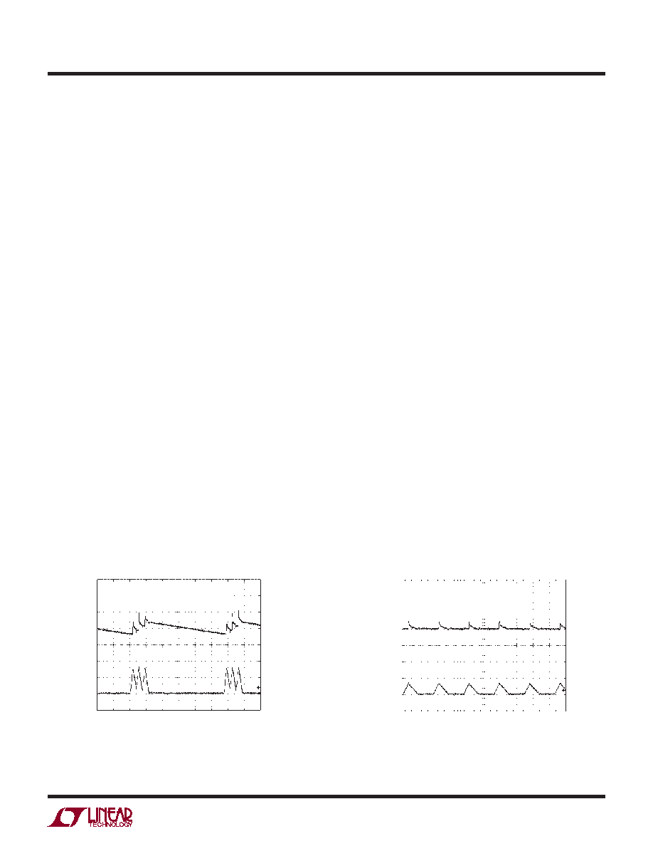
improving converter efciency. Oscilloscope waveforms
illustrating Burst Mode operation are shown in Figure 3.
Pulse-Skip Mode Operation
With the MODE/SYNC pin tied to a DC voltage above 2V,
Burst Mode operation is disabled. The internal, 0.525V
buffered ITH burst clamp is removed, allowing the ITH
pin to directly control the current comparator from no
load to full load. With no load, the ITH pin is driven below
0.175V, the power MOSFET is turned off and sleep mode
is invoked. Oscilloscope waveforms illustrating this mode
of operation are shown in Figure 4.
When an external clock signal drives the MODE/SYNC
pin at a rate faster than the chip’s internal oscillator, the
oscillator will synchronize to it. In this synchronized mode,
Burst Mode operation is disabled. The constant frequency
associated with synchronized operation provides a more
controlled noise spectrum from the converter, at the ex-
pense of overall system efciency of light loads.
Programming the Operating Mode
For applications where maximizing the efciency at very
light loads (e.g., <100μA) is a high priority, the current
in the output divider could be decreased to a few micro-
amps and Burst Mode operation should be applied (i.e.,
the MODE/SYNC pin should be connected to ground).
In applications where xed frequency operation is more
critical than low current efciency, or where the lowest
output ripple is desired, pulse-skip mode operation should
be used and the MODE/SYNC pin should be connected
to the INTVCC pin. This allows discontinuous conduction
mode (DCM) operation down to near the limit dened
by the chip’s minimum on-time (about 175ns). Below
this output current level, the converter will begin to skip
cycles in order to maintain output regulation. Figures 3
and 4 show the light load switching waveforms for Burst
Mode and pulse-skip mode operation for the converter
in Figure 1.
Burst Mode Operation
Burst Mode operation is selected by leaving the MODE/
SYNC pin unconnected or by connecting it to ground. In
normal operation, the range on the ITHpincorrespondingto
no load to full load is 0.30V to 1.2V. In Burst Mode opera-
tion, if the error amplier EA drives the ITH voltage below
0.525V, the buffered ITH input to the current comparator
C1 will be clamped at 0.525V (which corresponds to 25%
of maximum load current). The inductor current peak is
then held at approximately 30mV divided by the power
Figure 3. LTC1871-1 Burst Mode Operation
(MODE/SYNC = 0V) at Low Output Current
Figure 4. LTC1871-1 Low Output Current Operation with
Burst Mode Operation Disabled (MODE/SYNC = INTVCC)
VOUT
50mV/DIV
IL
5A/DIV
10μs/DIV
18711 F03
VIN = 3.3V
VOUT = 5V
IOUT = 500mA
MODE/SYNC = 0V
(Burst Mode OPERATION)
VOUT
50mV/DIV
IL
5A/DIV
2μs/DIV
18711 F04
VIN = 3.3V
VOUT = 5V
IOUT = 500mA
MODE/SYNC = INTVCC
(PULSE-SKIP MODE)
相關(guān)PDF資料 |
PDF描述 |
|---|---|
| LTC1871EMS-1#TR | SWITCHING CONTROLLER, 1000 kHz SWITCHING FREQ-MAX, PDSO10 |
| LTC2908IDDB8-B1 | 6-CHANNEL POWER SUPPLY SUPPORT CKT, PDSO8 |
| LTC2908CDDB8-B1#PBF | 6-CHANNEL POWER SUPPLY SUPPORT CKT, PDSO8 |
| LTC2908CDDB8-A1#PBF | 6-CHANNEL POWER SUPPLY SUPPORT CKT, PDSO8 |
| LTC2914IDHC-1#TR | 4-CHANNEL POWER SUPPLY SUPPORT CKT, PDSO16 |
相關(guān)代理商/技術(shù)參數(shù) |
參數(shù)描述 |
|---|---|
| LTC1871IMS-7 | 制造商:Linear Technology 功能描述:DP-SWREG/Controller, No Rsense DC/DC Controller Boost, Flyback & SEPIC |
| LTC1871IMS-7#PBF | 功能描述:IC REG CTRLR BST FLYBK CM 10MSOP RoHS:是 類別:集成電路 (IC) >> PMIC - 穩(wěn)壓器 - DC DC 切換控制器 系列:- 標(biāo)準(zhǔn)包裝:2,500 系列:- PWM 型:電流模式 輸出數(shù):1 頻率 - 最大:500kHz 占空比:96% 電源電壓:4 V ~ 36 V 降壓:無(wú) 升壓:是 回掃:無(wú) 反相:無(wú) 倍增器:無(wú) 除法器:無(wú) Cuk:無(wú) 隔離:無(wú) 工作溫度:-40°C ~ 125°C 封裝/外殼:24-WQFN 裸露焊盤(pán) 包裝:帶卷 (TR) |
| LTC1871IMS-7#TRPBF | 功能描述:IC REG CTRLR BST FLYBK CM 10MSOP RoHS:是 類別:集成電路 (IC) >> PMIC - 穩(wěn)壓器 - DC DC 切換控制器 系列:- 標(biāo)準(zhǔn)包裝:2,500 系列:- PWM 型:電流模式 輸出數(shù):1 頻率 - 最大:500kHz 占空比:96% 電源電壓:4 V ~ 36 V 降壓:無(wú) 升壓:是 回掃:無(wú) 反相:無(wú) 倍增器:無(wú) 除法器:無(wú) Cuk:無(wú) 隔離:無(wú) 工作溫度:-40°C ~ 125°C 封裝/外殼:24-WQFN 裸露焊盤(pán) 包裝:帶卷 (TR) |
| LTC1871IMSPBF | 制造商:Linear Technology 功能描述:PWM Controller Current Mode MSOP10 |
| LTC1872BES6 | 制造商:Linear Technology 功能描述:DC DC Cntrlr Single-OUT Step Up 2.5V to 9.8V Input 6-Pin TSOT-23 |
發(fā)布緊急采購(gòu),3分鐘左右您將得到回復(fù)。