- 您現(xiàn)在的位置:買賣IC網(wǎng) > PDF目錄10795 > LTC1382CSW#PBF (Linear Technology)IC TXRX 5V RS232 W/SHTDWN 18SOIC PDF資料下載
參數(shù)資料
| 型號: | LTC1382CSW#PBF |
| 廠商: | Linear Technology |
| 文件頁數(shù): | 5/8頁 |
| 文件大小: | 0K |
| 描述: | IC TXRX 5V RS232 W/SHTDWN 18SOIC |
| 標(biāo)準(zhǔn)包裝: | 40 |
| 類型: | 收發(fā)器 |
| 驅(qū)動器/接收器數(shù): | 2/2 |
| 規(guī)程: | RS232 |
| 電源電壓: | 4.5 V ~ 5 V |
| 安裝類型: | 表面貼裝 |
| 封裝/外殼: | 18-SOIC(0.295",7.50mm 寬) |
| 供應(yīng)商設(shè)備封裝: | 18-SOIC |
| 包裝: | 管件 |
| 產(chǎn)品目錄頁面: | 1354 (CN2011-ZH PDF) |
5
LTC1382
1382fa
VCC: 5V Input Supply Pin. This pin should be decoupled
with a 0.1F ceramic capacitor.
GND: Ground Pin.
ON/OFF: TTL/CMOS Compatible Shutdown Pin. A logic
low puts the device in the Shutdown mode. Both driver
outputs are forced into three-state and the supply current
is 0.2A.
V+: Positive Supply Output (RS232 Drivers). V+ 2VCC –
2V. This pin requires an external capacitor C = 0.1F for
charge storage. The capacitor may be tied to ground or
VCC. With multiple devices, the V + and V – pins may share
a common capacitor. For large numbers of devices, in-
creasing the size of the shared common storage capaci-
tors is recommended to reduce ripple.
V–: Negative Supply Output (RS232 Drivers). V – – (2VCC
– 2V). This pin requires an external capacitor C = 0.1F for
charge storage.
C1+, C1–, C2+, C2–: Commutating Capacitor Inputs. These
pins require two external capacitors C = 0.1F: one from
C1+ to C1– and another from C2+ to C2 –. To maintain
charge pump efficiency, the capacitor’s effective series
resistance should be less than 2.
TR IN: RS232 Driver Input Pins. Inputs are TTL/CMOS
compatible. The inputs of unused drivers can be left
unconnected since 300k input pull-up resistors to VCC are
included on chip. To minimize power consumption, the
internal driver pull-up resistors are disconnected from VCC
in the Shutdown mode.
TR OUT: Driver Outputs at RS232 Voltage Levels. Outputs
are in a high impedance state when in the Shutdown or
VCC = 0V. The driver outputs are protected against ESD to
±10kV for human body model discharges.
RX IN: Receiver Inputs. These pins can be forced to ±25V
without damage. The receiver inputs are protected against
ESD to ±10kV for human body model discharges. Each
receiver provides 0.4V of hysteresis for noise immunity.
RX OUT: Receiver Outputs with TTL/CMOS Voltage Lev-
els. Outputs are in a high impedance state when in the
Shutdown mode.
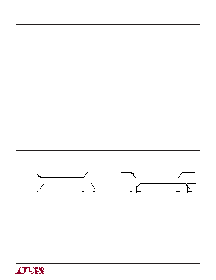
Figure 1. Driver Propagation Delay Timing
Figure 2. Receiver Propagation Delay Timing
SWITCHI G TI E WAVEFOR S
UW
W
1.4V
0V
VCC
0V
V+
V–
0V
DRIVER
INPUT
DRIVER
OUTPUT
1.4V
tHLD
tLHD
LTC1382 F01
0.8V
VCC
0V
2.4V
RX
INPUT
RX
OUTPUT
1.3V
tHLR
1.7V
tLHR
LTC1382 F02
VCC
0V
UU
U
PI FU CTIO S
發(fā)布緊急采購,3分鐘左右您將得到回復(fù)。