- 您現(xiàn)在的位置:買賣IC網(wǎng) > PDF目錄377733 > LTC1148 (Linear Technology Corporation) OCTAL BUS TRANSCEIVER O.C. 20-SOIC 0 to 70 PDF資料下載
參數(shù)資料
| 型號: | LTC1148 |
| 廠商: | Linear Technology Corporation |
| 英文描述: | OCTAL BUS TRANSCEIVER O.C. 20-SOIC 0 to 70 |
| 中文描述: | 高效率同步降壓型開關(guān)穩(wěn)壓器 |
| 文件頁數(shù): | 12/20頁 |
| 文件大?。?/td> | 384K |
| 代理商: | LTC1148 |
12
LTC1148
LTC1148-3.3/LTC1148-5
APPLICATIU
LTC1148 DC supply current is 160
μ
A for no load, and
increases proportionally with load up to a constant
1.6mA after the LTC1148 series has entered continu-
ous mode. Because the DC bias current is drawn from
V
IN
, the resulting loss increases with input voltage. For
V
IN
= 10V the DC bias losses are generally less than 1%
for load currents over 30mA. However, at very low load
currents the DC bias current accounts for nearly all of
the loss.
2. MOSFET gate charge current results from switching the
gate capacitance of the power MOSFETs. Each time a
MOSFET gate is switched from low to high to low again,
a packet of charge dQ moves from V
IN
to ground. The
resulting dQ/dt is a current out of V
IN
which is typically
much larger than the DC supply current. In continuous
mode, I
GATECHG
= f (Q
N
+ Q
P
). The typical gate charge
for a 0.1
N-channel power MOSFET is 25nC, and for
a P-channel about twice that value. This results in
I
GATECHG
= 7.5mA in 100kHz continuous operation, for
a 2% to 3% typical mid-current loss with V
IN
= 10V.
Note that the gate charge loss increases directly with
both input voltage and operating frequency. This is the
principal reason why the highest efficiency circuits
operate at moderate frequencies. Furthermore, it ar-
gues against using larger MOSFETs than necessary to
control I
2
R losses, since overkill can cost efficiency as
well as money!
3. I
2
R losses are easily predicted from the DC resistances
of the MOSFET, inductor, and current shunt. In continu-
ous mode the average output current flows through L
and R
SENSE
, but is “chopped” between the P-channel
and N-channel MOSFETs. If the two MOSFETs have
approximately the same R
DS(ON)
, then the resistance of
one MOSFET can simply be summed with the resis-
tances of L and R
SENSE
to obtain I
2
R losses. For
example, if each R
DS(ON)
= 0.1
, R
L
= 0.15
, and
R
SENSE
= 0.05
, then the total resistance is 0.3
. This
results in losses ranging from 3% to 12% as the output
current increases from 0.5A to 2A. I
2
R losses cause the
efficiency to roll-off at high output currents.
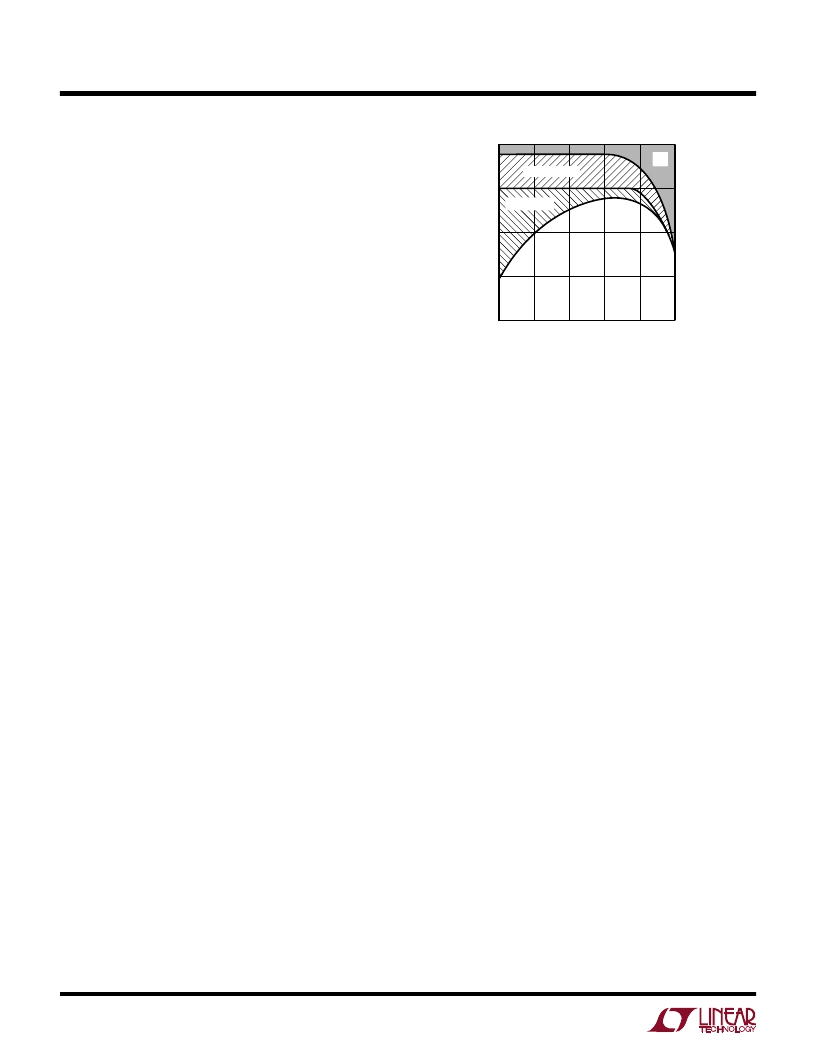
Figure 5 shows how the efficiency losses in a typical
LTC1148 series regulator end up being apportioned.
W
U
U
Figure 5. Efficiency Loss
OUTPUT CURRENT (A)
0.01
E
90
95
1
LTC1148 F05
85
80
0.03
0.1
0.3
3
100
GATE CHARGE
LTC1148 I
Q
I
2
R
The gate charge loss is responsible for the majority of
the efficiency lost in the mid-current region. If Burst
Mode operation was not employed at low currents, the
gate charge loss alone would cause efficiency to drop to
unacceptable levels. With Burst Mode
operation, the
DC supply current represents the lone (and unavoid-
able) loss component which continues to become a
higher percentage as output current is reduced. As
expected, the I
2
R losses dominate at high load currents.
Other losses including C
IN
and C
OUT
ESR dissipative
losses, MOSFET switching losses, Schottky conduction
losses during dead time, and inductor core losses, gener-
ally account for less than 2% total additional loss.
Design Example
As a design example, assume V
IN
= 12V (nominal),
V
OUT
= 5V, I
MAX
= 2A, and f = 200kHz; R
SENSE
, C
T
and L
can immediately be calculated:
R
SENSE
= 100mV/2 = 0.05
t
OFF
= (1/200kHz)[1 – (5/12)] = 2.92
μ
s
C
T
= 2.92
μ
s/[(1.3)(10
4
)] = 220pF
L
MIN
= 5.1
(
10
5
)0.05
(220pF)5V = 28
μ
H
Assume that the MOSFET dissipations are to be limited to
P
N
= P
P
= 250mW.
If T
A
= 50
°
C and the thermal resistance of each MOSFET
is 50
°
C/W, then the junction temperatures will be 63
°
C
相關(guān)PDF資料 |
PDF描述 |
|---|---|
| LTC1148HV | OCTAL BUS TRANSCEIVER O.C. 20-SOIC 0 to 70 |
| LTC1148L | OCTAL BUS TRANSCEIVER O.C. 20-SOIC 0 to 70 |
| LTC1148LCS | OCTAL BUS TRANSCEIVER O.C. 20-SOIC 0 to 70 |
| LTC1148HVCN-3.3 | RADIATION HARDENED HIGH EFFICIENCY, 5 AMP SWITCHING REGULATORS |
| LTC1148HVCN-5 | RADIATION HARDENED HIGH EFFICIENCY, 5 AMP SWITCHING REGULATORS |
相關(guān)代理商/技術(shù)參數(shù) |
參數(shù)描述 |
|---|---|
| LTC1148_04 | 制造商:LINER 制造商全稱:Linear Technology 功能描述:High Efficiency Synchronous Step-Down Switching Regulators |
| LTC1148-3.3 | 制造商:LINER 制造商全稱:Linear Technology 功能描述:High Efficiency Synchronous Step-Down Switching Regulators |
| LTC1148-5 | 制造商:LINER 制造商全稱:Linear Technology 功能描述:High Efficiency Synchronous Step-Down Switching Regulators |
| LTC1148CN | 功能描述:IC REG CTRLR BUCK PWM CM 14-DIP RoHS:否 類別:集成電路 (IC) >> PMIC - 穩(wěn)壓器 - DC DC 切換控制器 系列:- 標(biāo)準(zhǔn)包裝:4,500 系列:PowerWise® PWM 型:控制器 輸出數(shù):1 頻率 - 最大:1MHz 占空比:95% 電源電壓:2.8 V ~ 5.5 V 降壓:是 升壓:無 回掃:無 反相:無 倍增器:無 除法器:無 Cuk:無 隔離:無 工作溫度:-40°C ~ 125°C 封裝/外殼:6-WDFN 裸露焊盤 包裝:帶卷 (TR) 配用:LM1771EVAL-ND - BOARD EVALUATION LM1771 其它名稱:LM1771SSDX |
| LTC1148CN#PBF | 功能描述:IC REG CTRLR BUCK PWM CM 14-DIP RoHS:是 類別:集成電路 (IC) >> PMIC - 穩(wěn)壓器 - DC DC 切換控制器 系列:- 標(biāo)準(zhǔn)包裝:4,500 系列:PowerWise® PWM 型:控制器 輸出數(shù):1 頻率 - 最大:1MHz 占空比:95% 電源電壓:2.8 V ~ 5.5 V 降壓:是 升壓:無 回掃:無 反相:無 倍增器:無 除法器:無 Cuk:無 隔離:無 工作溫度:-40°C ~ 125°C 封裝/外殼:6-WDFN 裸露焊盤 包裝:帶卷 (TR) 配用:LM1771EVAL-ND - BOARD EVALUATION LM1771 其它名稱:LM1771SSDX |
發(fā)布緊急采購,3分鐘左右您將得到回復(fù)。