- 您現(xiàn)在的位置:買(mǎi)賣(mài)IC網(wǎng) > PDF目錄377724 > LTBDM (Linear Integrated Systems) Micropower Buck Regulator with Integrated Boost and Catch Diodes PDF資料下載
參數(shù)資料
| 型號(hào): | LTBDM |
| 廠商: | Linear Integrated Systems |
| 英文描述: | Micropower Buck Regulator with Integrated Boost and Catch Diodes |
| 中文描述: | 微功耗降壓穩(wěn)壓器與集成升壓二極管和捕捉 |
| 文件頁(yè)數(shù): | 12/16頁(yè) |
| 文件大?。?/td> | 205K |
| 代理商: | LTBDM |
第1頁(yè)第2頁(yè)第3頁(yè)第4頁(yè)第5頁(yè)第6頁(yè)第7頁(yè)第8頁(yè)第9頁(yè)第10頁(yè)第11頁(yè)當(dāng)前第12頁(yè)第13頁(yè)第14頁(yè)第15頁(yè)第16頁(yè)
12
LT3470
3470f
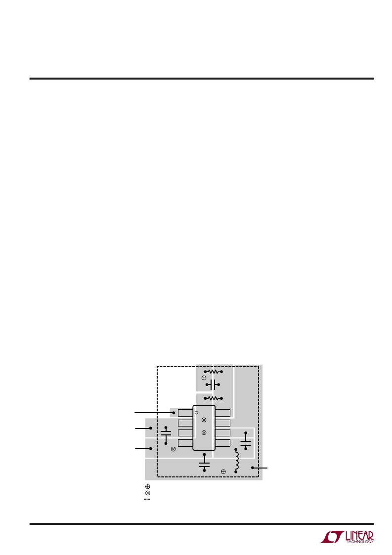
PCB Layout
For proper operation and minimum EMI, care must be
taken during printed circuit board layout. Note that large,
switched currents flow in the power switch, the internal
catch diode and the input capacitor. The loop formed by
these components should be as small as possible. Fur-
thermore, the system ground should be tied to the regu-
lator ground in only one place; this prevents the switched
current from injecting noise into the system ground.
These components, along with the inductor and output
capacitor, should be placed on the same side of the circuit
board, and their connections should be made on that layer.
Place a local, unbroken ground plane below these compo-
nents, and tie this ground plane to system ground at one
location, ideally at the ground terminal of the output
capacitor C2. Additionally, the SW and BOOST nodes
should be kept as small as possible. Unshielded inductors
can induce noise in the feedback path resulting in instabil-
ity and increased output ripple. To avoid this problem, use
vias to route the V
OUT
trace under the ground plane to the
feedback divider (as shown in Figure 5). Finally, keep the
FB node as small as possible so that the ground pin and
ground traces will shield it from the SW and BOOST nodes.
Figure 5 shows component placement with trace, ground
plane and via locations. Include vias near the GND pin of
the LT3470 to help remove heat from the LT3470 to the
ground plane.
Hot Plugging Safely
The small size, robustness and low impedance of ceramic
capacitors make them an attractive option for the input
bypass capacitor of LT3470. However, these capacitors
can cause problems if the LT3470 is plugged into a live
supply (see Linear Technology Application Note 88 for a
complete discussion). The low loss ceramic capacitor
combined with stray inductance in series with the power
source forms an under damped tank circuit, and the
voltage at the V
IN
pin of the LT3470 can ring to twice the
nominal input voltage, possibly exceeding the LT3470’s
rating and damaging the part. If the input supply is poorly
controlled or the user will be plugging the LT3470 into an
energized supply, the input network should be designed to
prevent this overshoot. Figure 6 shows the waveforms
that result when an LT3470 circuit is connected to a 24V
supply through six feet of 24-gauge twisted pair. The first
plot is the response with a 2.2
μ
F ceramic capacitor at the
input. The input voltage rings as high as 35V and the input
current peaks at 20A. One method of damping the tank
circuit is to add another capacitor with a series resistor to
the circuit. In Figure 6b an aluminum electrolytic capacitor
has been added. This capacitor’s high equivalent series
resistance damps the circuit and eliminates the voltage
overshoot. The extra capacitor improves low frequency
ripple filtering and can slightly improve the efficiency of
the circuit, though it is likely to be the largest component
Figure 5. A Good PCB Layout Ensures Proper, Low EMI Operation
SHDN
V
IN
V
OUT
3470 F05
GND
C1
C2
VIAS TO FEEDBACK DIVIDER
VIAS TO LOCAL GROUND PLANE
OUTLINE OF LOCAL GROUND PLANE
APPLICATIU
W
U
U
相關(guān)PDF資料 |
PDF描述 |
|---|---|
| LT3486 | Dual 1.3A White LED Step-Up Converters with Wide Dimming |
| LT3486EDHC | Dual 1.3A White LED Step-Up Converters with Wide Dimming |
| LT3486EFE | Dual 1.3A White LED Step-Up Converters with Wide Dimming |
| LT3524 | Regulating Pulse Width Modulator |
| LT3524N | Regulating Pulse Width Modulator |
相關(guān)代理商/技術(shù)參數(shù) |
參數(shù)描述 |
|---|---|
| LTBGB | 制造商:LINER 制造商全稱:Linear Technology 功能描述:Inverting 1.2MHz/2.7MHz DC/DC Converters with Integrated Schottky in ThinSOT |
| LTBGP | 制造商:LINER 制造商全稱:Linear Technology 功能描述:Serial 12-Bit/14-Bit, 2.8Msps Sampling ADCs with Shutdown |
| LTBGQ | 制造商:LINER 制造商全稱:Linear Technology 功能描述:Serial 12-Bit/14-Bit, 2.8Msps Sampling ADCs with Shutdown |
| LTBGR | 制造商:LINER 制造商全稱:Linear Technology 功能描述:Serial 12-Bit/14-Bit, 2.8Msps Sampling ADCs with Shutdown |
| LTBGS | 制造商:LINER 制造商全稱:Linear Technology 功能描述:Serial 12-Bit/14-Bit, 2.8Msps Sampling ADCs with Shutdown |
發(fā)布緊急采購(gòu),3分鐘左右您將得到回復(fù)。