- 您現在的位置:買賣IC網 > PDF目錄39400 > LT6350IMS8#PBF (LINEAR TECHNOLOGY CORP) 1-CH 16-BIT SUCCESSIVE APPROXIMATION ADC, PARALLEL ACCESS, PDSO8 PDF資料下載
參數資料
| 型號: | LT6350IMS8#PBF |
| 廠商: | LINEAR TECHNOLOGY CORP |
| 元件分類: | ADC |
| 英文描述: | 1-CH 16-BIT SUCCESSIVE APPROXIMATION ADC, PARALLEL ACCESS, PDSO8 |
| 封裝: | LEAD FREE, PLASTIC, MSOP-8 |
| 文件頁數: | 8/28頁 |
| 文件大小: | 462K |
| 代理商: | LT6350IMS8#PBF |
第1頁第2頁第3頁第4頁第5頁第6頁第7頁當前第8頁第9頁第10頁第11頁第12頁第13頁第14頁第15頁第16頁第17頁第18頁第19頁第20頁第21頁第22頁第23頁第24頁第25頁第26頁第27頁第28頁
LT6350
16
6350fb
APPLICATIONS INFORMATION
Driving the input signal sufciently beyond the power
supply rails will cause the input transistors to saturate.
When saturation occurs, the amplier loses a stage of
phase inversion and the output tries to invert. Diodes D1
and D2 (Figure 5) forward bias and hold the output within
a diode drop of the input signal. With very heavy input
overdrive the output of op amp 1 could invert. To avoid
this inversion, limit the input overdrive to 0.5V beyond
the power supply rails.
OUTPUT VOLTAGE RANGE
The outputs of the LT6350 typically swing to within 55mV
of the upper and lower supply rails when driving a purely
capacitive load such as at the switched-capacitor input
stage of a SAR ADC. The LT6350 can therefore share a
single 5V supply with the SAR ADC and drive a full 8VP-P
differential around an input common mode voltage between
2.055V and 2.945V. A modest negative supply can be
added to allow the LT6350 to swing all the way to 0V in
systems where the ADC requires a true 0V-referenced
signal or when the input common mode range of the ADC
is restricted to be lower than 2.055V. Some SAR ADCs use
2V as the input common mode voltage with a full-scale
input signal range at each input of 0V to 4V. The outputs
of the LT6350 can swing 7.78VP-P differentially around a
2V common mode voltage, which is a loss of only 0.24dB
of the full-scale range of such ADCs.
+
–
+IN1
–IN1
V+
V–
OUT2
OUT1
SHDN
+IN2
VIN
5V
0.1μF
2V
LT6350
6350 F06
+
–
CCM
RS
RFILT
RS
CDIFF
CCM
+
–
AIN
+
AIN
–
ADC
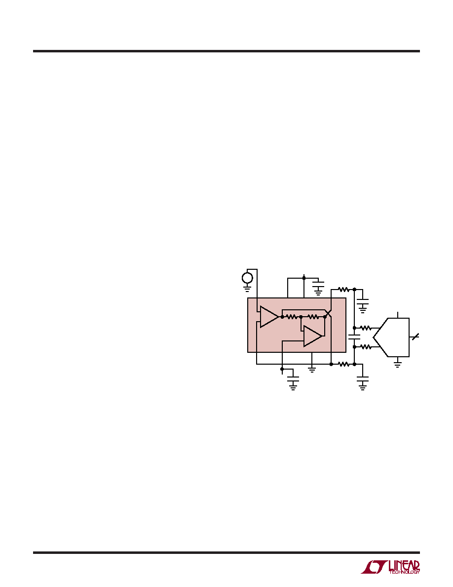
Figure 6. Driving an ADC
INTERFACING THE LT6350 TO A/D CONVERTERS
When driving an ADC, an additional single-pole passive
RC lter added between the outputs of the LT6350 and
the inputs of the ADC can sometimes improve system
performance. This is because the sampling process of ADCs
creates a charge transient at the ADC inputs that is caused
by the switching in of the ADC sampling capacitor. This
momentarily shorts the output of the amplier as charge is
transferred between amplier and sampling capacitor. For
an accurate representation of the input signal, the amplier
must recover and settle from this load transient before
the acquisition period has ended. An RC network at the
outputs of the driver helps decouple the sampling transient
of the ADC from the amplier reducing the demands on
the amplier’s output stage (see Figure 6). The resistors
at the inputs to the ADC minimize the sampling transients
that charge the RC lter capacitors.
相關PDF資料 |
PDF描述 |
|---|---|
| LT6350CMS8#TRPBF | 1-CH 16-BIT SUCCESSIVE APPROXIMATION ADC, PARALLEL ACCESS, PDSO8 |
| LT6350HDD#PBF | 1-CH 16-BIT SUCCESSIVE APPROXIMATION ADC, PARALLEL ACCESS, PDSO8 |
| LT6350HMS8#PBF | 1-CH 16-BIT SUCCESSIVE APPROXIMATION ADC, PARALLEL ACCESS, PDSO8 |
| LT6350CDD#PBF | 1-CH 16-BIT SUCCESSIVE APPROXIMATION ADC, PARALLEL ACCESS, PDSO8 |
| LT6604IUFF-15#TRPBF | SPECIALTY ANALOG CIRCUIT, PQCC34 |
相關代理商/技術參數 |
參數描述 |
|---|---|
| LT6350IMS8TRPBF | 制造商:LINER 制造商全稱:Linear Technology 功能描述:Low Noise Single-Ended to Differential Converter/ADC Driver |
| LT6360 | 制造商:LINER 制造商全稱:Linear Technology 功能描述:18-Bit, 1.6Msps, Pseudo-Differential Unipolar SAR |
| LT63H-SERIES | 制造商:未知廠家 制造商全稱:未知廠家 功能描述:Optoelectronic |
| LT63HXX-SERIES | 制造商:未知廠家 制造商全稱:未知廠家 功能描述:Optoelectronic |
| LT6402-12 | 制造商:LINER 制造商全稱:Linear Technology 功能描述:1.3GHz Low Noise, Low Distortion Differential ADC Driver for 140MHz IF |
發(fā)布緊急采購,3分鐘左右您將得到回復。