- 您現(xiàn)在的位置:買賣IC網(wǎng) > PDF目錄30767 > LT3695IMSE-5#PBF (LINEAR TECHNOLOGY CORP) 2 A SWITCHING REGULATOR, 2420 kHz SWITCHING FREQ-MAX, PDSO16 PDF資料下載
參數(shù)資料
| 型號(hào): | LT3695IMSE-5#PBF |
| 廠商: | LINEAR TECHNOLOGY CORP |
| 元件分類: | 穩(wěn)壓器 |
| 英文描述: | 2 A SWITCHING REGULATOR, 2420 kHz SWITCHING FREQ-MAX, PDSO16 |
| 封裝: | LEAD FREE, PLASTIC, MSOP-16 |
| 文件頁(yè)數(shù): | 25/30頁(yè) |
| 文件大?。?/td> | 491K |
| 代理商: | LT3695IMSE-5#PBF |
第1頁(yè)第2頁(yè)第3頁(yè)第4頁(yè)第5頁(yè)第6頁(yè)第7頁(yè)第8頁(yè)第9頁(yè)第10頁(yè)第11頁(yè)第12頁(yè)第13頁(yè)第14頁(yè)第15頁(yè)第16頁(yè)第17頁(yè)第18頁(yè)第19頁(yè)第20頁(yè)第21頁(yè)第22頁(yè)第23頁(yè)第24頁(yè)當(dāng)前第25頁(yè)第26頁(yè)第27頁(yè)第28頁(yè)第29頁(yè)第30頁(yè)
LT3695 Series
4
3695fa
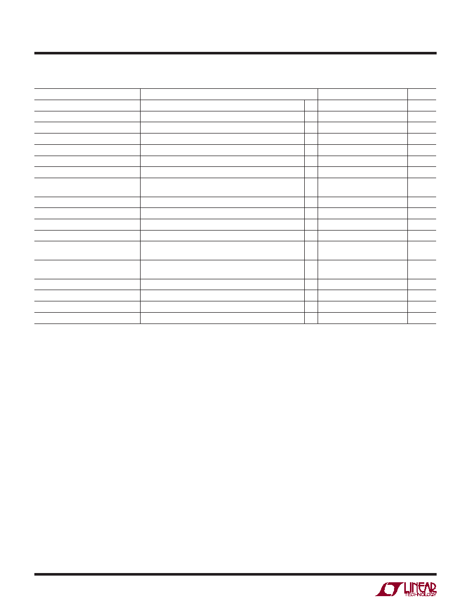
ELECTRICAL CHARACTERISTICS The l denotes the specications which apply over the full operating
temperature range, otherwise specications are at TA = 25°C. VIN = 10V, VRUN/SS = 10V, unless otherwise noted. (Note 4)
PARAMETER
CONDITIONS
MIN
TYP
MAX
UNITS
Switch VCESAT
ISW = 1A
350
mV
DA Pin Current to Stop OSC
1.25
1.6
1.95
A
Switch Leakage Current
VSW = 0V, VIN = 36V
0.01
1
μA
Boost Schottky Diode Voltage Drop
IBSD = 50mA
720
900
mV
Boost Schottky Diode Reverse Leakage
VSW = 10V, VBD = 0V
0.1
1
μA
Minimum Boost Voltage (Note 8)
l
1.7
2.3
V
BOOST Pin Current
ISW = 0.5A
10.5
17.5
mA
RUN/SS Pin Current
VRUN/SS = 2.5V
VRUN/SS = 10V
l
4.5
12
7.5
20
μA
RUN/SS Input Voltage High
2.5
V
RUN/SS Input Voltage Low
0.2
V
PG Leakage Current
VPG = 5V
0.1
1
μA
PG Sink Current
VPG = 0.4V
l
100
1000
μA
PG Threshold as % of VFB (LT3695) or
VOUT (LT3695-3.3, LT3695-5)
Measured at FB (LT3695) or OUT1,2 (LT3695-3.3, LT3695-5)
Pins (Pin Voltage Rising)
88
90
92
%
PG Threshold Hysteresis
LT3695
Measured at FB Pin
12
mV
LT3695-3.3 Measured at OUT1,2, Pins
50
mV
LT3695-5
Measured at OUT1,2, Pins
75
mV
SYNC Threshold Voltage
300
550
800
mV
SYNC Input Frequency
0.3
2.2
MHz
Note 1: Stresses beyond those listed under absolute maximum ratings
may cause permanent damage to the device. Exposure to any Absolute
Maximum Rating condition for extended periods may affect the device
reliability and lifetime.
Note 2: Positive currents ow into pins, negative currents ow out of pins.
Minimum and maximum values refer to absolute values.
Note 3: Absolute maximum voltage at VIN and RUN/SS pins is 60V for
nonrepetitive 1 second transients, and 36V for continuous operation.
Note 4: The LT3695E regulators are guaranteed to meet performance
specications from 0°C to 125°C junction temperature. Specications
over the –40°C to 125°C operating junction temperature range are
assured by design, characterization and correlation with statistical process
controls. The LT3695I regulators are guaranteed over the full –40°C to
125°C operating junction temperature range. The LT3695H regulators are
guaranteed over the full –40°C to 150°C operating junction temperature
range.
Note 5: These ICs include overtemperature protection that is intended
to protect the devices during momentary overload conditions. Junction
temperature will exceed the maximum operating junction temperature
when overtemperature protection is active. Continuous operation above
the specied maximum operating junction temperature may impair device
reliability.
Note 6: This is the voltage necessary to keep the internal bias circuitry in
regulation.
Note 7: Current limit guaranteed by design and/or correlation to static test.
Slope compensation reduces current limit at higher duty cycles.
Note 8: This is the minimum voltage across the boost capacitor needed to
guarantee full saturation of the switch.
相關(guān)PDF資料 |
PDF描述 |
|---|---|
| LT3695EMSE-5#TRPBF | 2 A SWITCHING REGULATOR, 2420 kHz SWITCHING FREQ-MAX, PDSO16 |
| LT3695IMSE-5#TRPBF | 2 A SWITCHING REGULATOR, 2420 kHz SWITCHING FREQ-MAX, PDSO16 |
| LT3695EMSE-3.3#PBF | 2 A SWITCHING REGULATOR, 2420 kHz SWITCHING FREQ-MAX, PDSO16 |
| LT3695EMSE-3.3#TRPBF | 2 A SWITCHING REGULATOR, 2420 kHz SWITCHING FREQ-MAX, PDSO16 |
| LT3751IUFD#TR | 1-CHANNEL POWER SUPPLY SUPPORT CKT, PQCC20 |
相關(guān)代理商/技術(shù)參數(shù) |
參數(shù)描述 |
|---|---|
| LT3695IMSEPBF | 制造商:LINER 制造商全稱:Linear Technology 功能描述:1A Fault Tolerant Micropower Step-Down Regulator |
| LT3695IMSETRPBF | 制造商:LINER 制造商全稱:Linear Technology 功能描述:1A Fault Tolerant Micropower Step-Down Regulator |
| LT370 | 功能描述:標(biāo)準(zhǔn)LED-通孔 Green RoHS:否 制造商:Vishay Semiconductors 照明顏色:Red 光強(qiáng)度:0.7 mcd 波長(zhǎng)/色溫:615 nm 顯示角:45 deg 透鏡顏色/類型:Clear, Non-Diffused 正向電流:70 mA 正向電壓:1.83 V to 3.03 V LED 大小:2 mm 系列: 封裝:Tube |
| LT370_1 | 制造商:SEOUL 制造商全稱:Seoul Semiconductor 功能描述:GREEN LAMP LED |
| LT370Z | 制造商:SEOUL 制造商全稱:Seoul Semiconductor 功能描述:GREEN OVAL LAMP LED |
發(fā)布緊急采購(gòu),3分鐘左右您將得到回復(fù)。