- 您現(xiàn)在的位置:買(mǎi)賣(mài)IC網(wǎng) > PDF目錄67757 > LT3493EDCB#PBF (LINEAR TECHNOLOGY CORP) 2.2 A SWITCHING REGULATOR, 815 kHz SWITCHING FREQ-MAX, PDSO6 PDF資料下載
參數(shù)資料
| 型號(hào): | LT3493EDCB#PBF |
| 廠商: | LINEAR TECHNOLOGY CORP |
| 元件分類(lèi): | 穩(wěn)壓器 |
| 英文描述: | 2.2 A SWITCHING REGULATOR, 815 kHz SWITCHING FREQ-MAX, PDSO6 |
| 封裝: | 2 X 3 MM, LEAD FREE, PLASTIC, MO-229, DFN-6 |
| 文件頁(yè)數(shù): | 8/20頁(yè) |
| 文件大?。?/td> | 588K |
| 代理商: | LT3493EDCB#PBF |
第1頁(yè)第2頁(yè)第3頁(yè)第4頁(yè)第5頁(yè)第6頁(yè)第7頁(yè)當(dāng)前第8頁(yè)第9頁(yè)第10頁(yè)第11頁(yè)第12頁(yè)第13頁(yè)第14頁(yè)第15頁(yè)第16頁(yè)第17頁(yè)第18頁(yè)第19頁(yè)第20頁(yè)
LT3493
16
3493fb
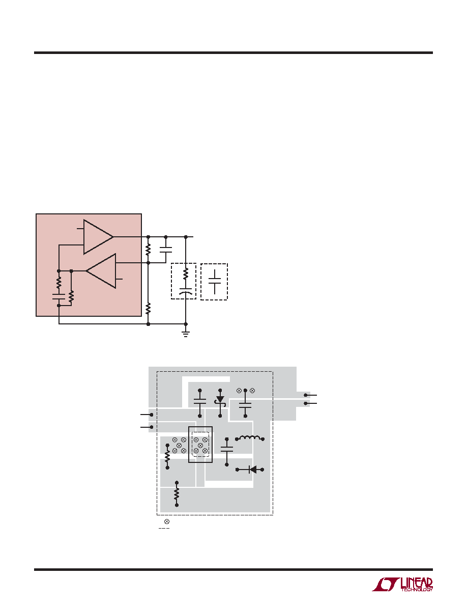
model works well as long as the value of the inductor is
not too high and the loop crossover frequency is much
lower than the switching frequency. With a larger ceramic
capacitor (very low ESR), crossover may be lower and a
phase lead capacitor (CPL) across the feedback divider may
improve the phase margin and transient response. Large
electrolytic capacitors may have an ESR large enough to
create an additional zero, and the phase lead may not be
necessary.
If the output capacitor is different than the recommended
capacitor, stability should be checked across all operating
conditions, including load current, input voltage and tem-
perature. The LT1375 data sheet contains a more thorough
discussion of loop compensation and describes how to
test the stability using a transient load.
PCB Layout
For proper operation and minimum EMI, care must be taken
during printed circuit board layout. Figure 11 shows the
recommended component placement with trace, ground
plane and via locations. Note that large, switched currents
ow in the LT3493’s VIN and SW pins, the catch diode (D1)
and the input capacitor (C2). The loop formed by these
components should be as small as possible and tied to
system ground in only one place. These components, along
with the inductor and output capacitor, should be placed on
the same side of the circuit board, and their connections
should be made on that layer. Place a local, unbroken ground
plane below these components, and tie this ground plane
to system ground at one location, ideally at the ground
terminal of the output capacitor C1. The SW and BOOST
nodes should be as small as possible. Finally, keep the
FB node small so that the ground pin and ground traces
will shield it from the SW and BOOST nodes. Include vias
near the exposed GND pad of the LT3493 to help remove
heat from the LT3493 to the ground plane.
APPLICATIONS INFORMATION
–
+
–
+
780mV
SW
VC
LT3493
GND
3493 F10
R1
OUT
ESR
ERROR
AMPLIFIER
CURRENT MODE
POWER STAGE
FB
R2
1M
RC
60k
CC
100pF
C1
gm =
300μA/V
gm =
1.6A/V
+
CPL
0.7V
Figure 10. Model for Loop Response
Figure 11. A Good PCB Layout Ensures Proper, Low EMI Operation
C2
D1
C1
SYSTEM
GROUND
: VIAS TO LOCAL GROUND PLANE
: OUTLINE OF LOCAL GROUND PLANE
VOUT
3493 F11
VIN
SHDN
相關(guān)PDF資料 |
PDF描述 |
|---|---|
| LT3493IDCB#PBF | 2.2 A SWITCHING REGULATOR, 815 kHz SWITCHING FREQ-MAX, PDSO6 |
| LT3493EDCB#TRM | 2.2 A SWITCHING REGULATOR, 815 kHz SWITCHING FREQ-MAX, PDSO6 |
| LT3493EDCB#TR | 2.2 A SWITCHING REGULATOR, 815 kHz SWITCHING FREQ-MAX, PDSO6 |
| LT3513EUHF#TRPBF | 3.5 A SWITCHING REGULATOR, 2220 kHz SWITCHING FREQ-MAX, PQCC38 |
| LT3513EUHF#PBF | 3.5 A SWITCHING REGULATOR, 2220 kHz SWITCHING FREQ-MAX, PQCC38 |
相關(guān)代理商/技術(shù)參數(shù) |
參數(shù)描述 |
|---|---|
| LT3493EDCB-TR | 制造商:LINER 制造商全稱(chēng):Linear Technology 功能描述:1.2A, 750kHz Step-Down Switching Regulator in 2mm × 3mm DFN |
| LT3493EDCBTRMPBF | 制造商:Linear Technology 功能描述:Sw. Regulator 1.2A 750kHz Step-Down DFN6 |
| LT3493EDCB-TRPBF | 制造商:LINER 制造商全稱(chēng):Linear Technology 功能描述:1.2A, 750kHz Step-Down Switching Regulator in 2mm × 3mm DFN |
| LT3493IDCB | 制造商:LINER 制造商全稱(chēng):Linear Technology 功能描述:1.2A, 750kHz Step-Down Switching Regulator in 2mm × 3mm DFN |
| LT3493IDCB#PBF | 制造商:Linear Technology 功能描述:BUCK SW REG 1.4A 750KHZ 6D 制造商:Linear Technology 功能描述:DC-DC CONVERTER BUCK 750KHZ 制造商:Linear Technology 功能描述:BUCK, SW REG, 1.4A, 750KHZ, 6DFN 制造商:Linear Technology 功能描述:DC-DC CONVERTER, BUCK, 750KHZ, 1.2A, DFN-6; Primary Input Voltage:36V; No. of Outputs:1; Output Voltage:780mV; Output Current:1.2A; No. of Pins:6; Operating Temperature Min:-40C; Operating Temperature Max:125C; Package / Case:6-DFN;RoHS Compliant: Yes |
發(fā)布緊急采購(gòu),3分鐘左右您將得到回復(fù)。