- 您現(xiàn)在的位置:買賣IC網(wǎng) > PDF目錄30767 > LT3470ITS8#PBF (LINEAR TECHNOLOGY CORP) 0.2 A SWITCHING REGULATOR, PDSO8 PDF資料下載
參數(shù)資料
| 型號: | LT3470ITS8#PBF |
| 廠商: | LINEAR TECHNOLOGY CORP |
| 元件分類: | 穩(wěn)壓器 |
| 英文描述: | 0.2 A SWITCHING REGULATOR, PDSO8 |
| 封裝: | 1 MM HEIGHT, LEAD FREE, PLASTIC, MO-193, SOT-23, 8 PIN |
| 文件頁數(shù): | 5/20頁 |
| 文件大小: | 256K |
| 代理商: | LT3470ITS8#PBF |
13
LT3470
3470fc
SHDN
VIN
VOUT
(A)
(B)
VOUT
3470 F05
GND
SHDN
VIN
GND
C1
C2
VIAS TO FEEDBACK DIVIDER
VIAS TO LOCAL GROUND PLANE
OUTLINE OF LOCAL GROUND PLANE
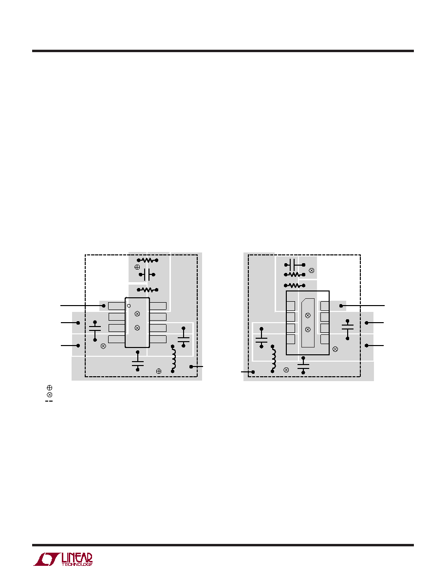
PCB Layout
For proper operation and minimum EMI, care must be
taken during printed circuit board layout. Note that large,
switched currents flow in the power switch, the internal
catch diode and the input capacitor. The loop formed by
these components should be as small as possible. Fur-
thermore, the system ground should be tied to the regu-
lator ground in only one place; this prevents the switched
current from injecting noise into the system ground.
These components, along with the inductor and output
capacitor, should be placed on the same side of the circuit
board, and their connections should be made on that layer.
Place a local, unbroken ground plane below these compo-
nents, and tie this ground plane to system ground at one
Figure 5. A Good PCB Layout Ensures Proper, Low EMI Operation
APPLICATIO S I FOR ATIO
WU
UU
location, ideally at the ground terminal of the output
capacitor C2. Additionally, the SW and BOOST nodes
should be kept as small as possible. Unshielded inductors
can induce noise in the feedback path resulting in instabil-
ity and increased output ripple. To avoid this problem, use
vias to route the VOUT trace under the ground plane to the
feedback divider (as shown in Figure 5). Finally, keep the
FB node as small as possible so that the ground pin and
ground traces will shield it from the SW and BOOST nodes.
Figure 5 shows component placement with trace, ground
plane and via locations. Include vias near the GND pin, or
pad, of the LT3470 to help remove heat from the LT3470
to the ground plane.
相關(guān)PDF資料 |
PDF描述 |
|---|---|
| LT3470HTS8#TR | SWITCHING REGULATOR, PDSO8 |
| LT3495BEDDB#PBF | 0.78 A SWITCHING REGULATOR, PDSO10 |
| LT3495BEDDB-1#PBF | 0.45 A SWITCHING REGULATOR, PDSO10 |
| LT3495EDDB-1#PBF | 0.45 A SWITCHING REGULATOR, PDSO10 |
| LT3495EDDB-1#TRMPBF | 0.45 A SWITCHING REGULATOR, PDSO10 |
相關(guān)代理商/技術(shù)參數(shù) |
參數(shù)描述 |
|---|---|
| LT3470ITS8TRMPBF | 制造商:Linear Technology 功能描述:DC-DC Converter Step-Down 4-40V TSOT23-8 |
| LT3471 | 制造商:LINER 制造商全稱:Linear Technology 功能描述:Dual 1.3A, 1.2MHz Boost/Inverter in 3mm ???? 3mm DFN |
| LT3471EDD | 制造商:Linear Technology 功能描述:Conv DC-DC Dual Inv/Step Up 2.4V to 16V 10-Pin DFN EP |
| LT3471EDD#PBF | 功能描述:IC REG MULTI CONFIG ADJ DL 10DFN RoHS:是 類別:集成電路 (IC) >> PMIC - 穩(wěn)壓器 - DC DC 開關(guān)穩(wěn)壓器 系列:- 標(biāo)準(zhǔn)包裝:250 系列:- 類型:降壓(降壓) 輸出類型:固定 輸出數(shù):1 輸出電壓:1.2V 輸入電壓:2.05 V ~ 6 V PWM 型:電壓模式 頻率 - 開關(guān):2MHz 電流 - 輸出:500mA 同步整流器:是 工作溫度:-40°C ~ 85°C 安裝類型:表面貼裝 封裝/外殼:6-UFDFN 包裝:帶卷 (TR) 供應(yīng)商設(shè)備封裝:6-SON(1.45x1) 產(chǎn)品目錄頁面:1032 (CN2011-ZH PDF) 其它名稱:296-25628-2 |
| LT3471EDD#PBF | 制造商:Linear Technology 功能描述:DC/DC Converter IC 制造商:Linear Technology 功能描述:IC, DUAL BOOST/INVERTER REGULATOR, DFN10 |
發(fā)布緊急采購,3分鐘左右您將得到回復(fù)。