- 您現(xiàn)在的位置:買賣IC網(wǎng) > PDF目錄39399 > LT3407EDD-2#TR (LINEAR TECHNOLOGY CORP) 1.6 A DUAL SWITCHING CONTROLLER, 2700 kHz SWITCHING FREQ-MAX, PDSO10 PDF資料下載
參數(shù)資料
| 型號: | LT3407EDD-2#TR |
| 廠商: | LINEAR TECHNOLOGY CORP |
| 元件分類: | 穩(wěn)壓器 |
| 英文描述: | 1.6 A DUAL SWITCHING CONTROLLER, 2700 kHz SWITCHING FREQ-MAX, PDSO10 |
| 封裝: | 3 X 3 MM, PLASTIC, MO-229WEED-2, DFN-10 |
| 文件頁數(shù): | 12/16頁 |
| 文件大小: | 221K |
| 代理商: | LT3407EDD-2#TR |
LTC3407-2
5
34072fa
VFB1 (Pin 1): Output Feedback. Receives the feedback
voltage from the external resistive divider across the
output. Nominal voltage for this pin is 0.6V.
RUN1 (Pin 2): Regulator 1 Enable. Forcing this pin to VIN
enables regulator 1, while forcing it to GND causes regu-
lator 1 to shut down.
VIN (Pin 3): Main Power Supply. Must be closely decoupled
to GND.
SW1 (Pin 4): Regulator 1 Switch Node Connection to the
Inductor. This pin swings from VIN to GND.
GND (Pin 5): Main Ground. Connect to the (–) terminal of
COUT, and (–) terminal of CIN.
MODE/SYNC (Pin 6): Combination Mode Selection and
Oscillator Synchronization. This pin controls the operation
of the device. When tied to VIN or GND, Burst Mode
operation or pulse skipping mode is selected, respec-
tively. Do not float this pin. The oscillation frequency can
UU
U
PI FU CTIO S
be syncronized to an external oscillator applied to this pin
and pulse skipping mode is automatically selected.
SW2 (Pin 7): Regulator 2 Switch Node Connection to the
Inductor. This pin swings from VIN to GND.
POR (Pin 8): Power-On Reset . This common-drain logic
output is pulled to GND when the output voltage is not
within
±8.5% of regulation and goes high after 117ms
when both channels are within regulation.
RUN2 (Pin 9): Output Feedback. Forcing this pin to VIN
enables regulator 2, while forcing it to GND causes regu-
lator 2 to shut down.
VFB2 (Pin 10): Output Feedback. Receives the feedback
voltage from the external resistive divider across the
output. Nominal voltage for this pin is 0.6V.
Exposed Pad (GND) (Pin 11): Power Ground. Connect to
the (–) terminal of COUT, and (–) terminal of CIN. Must be
connected to electrical ground on PCB.
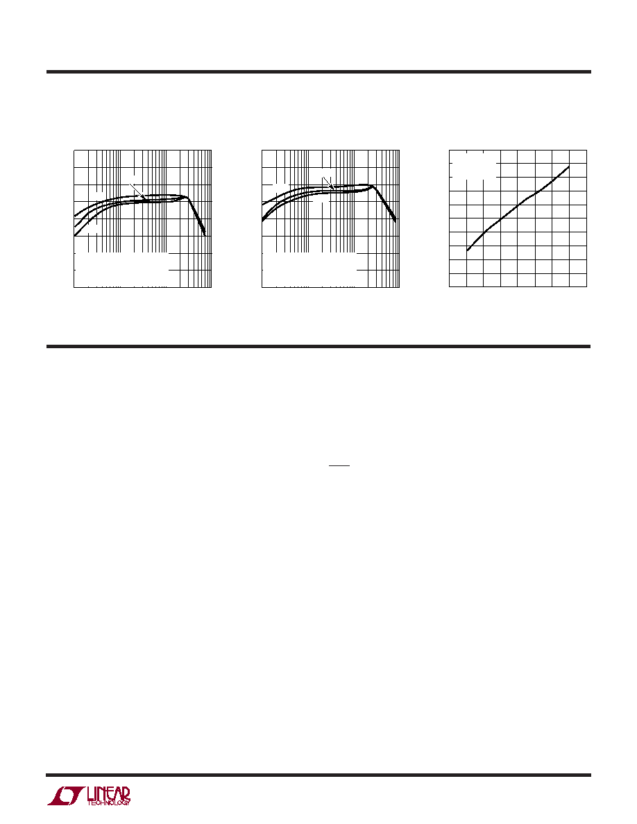
TYPICAL PERFOR A CE CHARACTERISTICS
UW
VIN (V)
2
V
OUT
ERROR
(%)
0.5
0.4
0.3
0.2
0.1
0
–0.1
–0.2
–0.3
–0.4
–0.5
4
6
3407 G15
35
VOUT = 1.8V
IOUT = 200mA
TA = 25°C
LOAD CURRENT (mA)
1
EFFICIENCY
(%)
100
95
90
85
80
75
70
65
60
10
100
1000
3407 G13
2.7V
4.2V
VOUT = 1.2V
Burst Mode OPERATION
NO LOAD ON OTHER CHANNEL
CIRCUIT OF FIGURE 1
LOAD CURRENT (mA)
1
EFFICIENCY
(%)
100
95
90
85
80
75
70
65
60
10
100
1000
3407 G14
2.7V
4.2V
VOUT = 1.5V
Burst Mode OPERATION
NO LOAD ON OTHER CHANNEL
CIRCUIT OF FIGURE 1
3.6V
Efficiency vs Load Current
Line Regulation
TA = 25°C unless other wise specified.
相關PDF資料 |
PDF描述 |
|---|---|
| LT3500HMSE#PBF | 3.5 A SWITCHING REGULATOR, 2800 kHz SWITCHING FREQ-MAX, PDSO16 |
| LT3500HMSE#TRPBF | 3.5 A SWITCHING REGULATOR, 2800 kHz SWITCHING FREQ-MAX, PDSO16 |
| LT3500IMSE#TRPBF | 3.5 A SWITCHING REGULATOR, 2800 kHz SWITCHING FREQ-MAX, PDSO16 |
| LT3757MPMSE#TRPBF | SWITCHING REGULATOR, 1000 kHz SWITCHING FREQ-MAX, PDSO10 |
| LT3757HMSE#TRPBF | SWITCHING REGULATOR, 1000 kHz SWITCHING FREQ-MAX, PDSO10 |
相關代理商/技術參數(shù) |
參數(shù)描述 |
|---|---|
| LT340Z | 制造商:SEOUL 制造商全稱:Seoul Semiconductor 功能描述:GREEN OVAL LAMP LED |
| LT341 | 制造商:SEOUL 制造商全稱:Seoul Semiconductor 功能描述:BLUE OVAL LAMP LED |
| LT3412G | 制造商:未知廠家 制造商全稱:未知廠家 功能描述:Optoelectronic |
| LT341BC | 制造商:Datak Corporation 功能描述: |
| LT341L | 制造商:未知廠家 制造商全稱:未知廠家 功能描述:Optoelectronic |
發(fā)布緊急采購,3分鐘左右您將得到回復。