- 您現(xiàn)在的位置:買賣IC網(wǎng) > PDF目錄44983 > LT1871EMS-7#TR (LINEAR TECHNOLOGY CORP) SWITCHING CONTROLLER, 1000 kHz SWITCHING FREQ-MAX, PDSO10 PDF資料下載
參數(shù)資料
| 型號: | LT1871EMS-7#TR |
| 廠商: | LINEAR TECHNOLOGY CORP |
| 元件分類: | 穩(wěn)壓器 |
| 英文描述: | SWITCHING CONTROLLER, 1000 kHz SWITCHING FREQ-MAX, PDSO10 |
| 封裝: | PLASTIC, MSOP-10 |
| 文件頁數(shù): | 27/32頁 |
| 文件大?。?/td> | 461K |
| 代理商: | LT1871EMS-7#TR |
第1頁第2頁第3頁第4頁第5頁第6頁第7頁第8頁第9頁第10頁第11頁第12頁第13頁第14頁第15頁第16頁第17頁第18頁第19頁第20頁第21頁第22頁第23頁第24頁第25頁第26頁當(dāng)前第27頁第28頁第29頁第30頁第31頁第32頁

LTC1871-7
4
18717fc
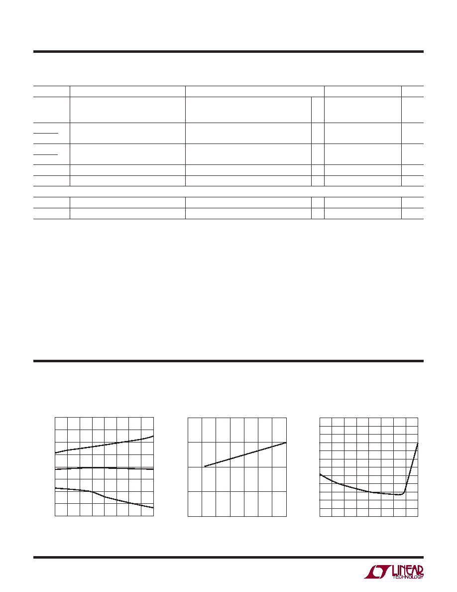
FB Voltage vs Temp
FB Voltage Line Regulation
FB Pin Current vs Temperature
ELECTRICAL CHARACTERISTICS The l denotes the specications which apply over the full operating
temperature range, otherwise specications are at TA = 25°C. VIN = 8V, VRUN = 1.5V, RFREQ = 80k, VMODE/SYNC = 0V, unless otherwise specied.
SYMBOL
PARAMETER
CONDITIONS
MIN
TYP
MAX
UNITS
UVLO
INTVCC Undervoltage Lockout Threshold
Rising INTVCC
Falling INTVCC
UVLO Hysteresis
5.6
4.6
1.0
V
ΔVINTVCC
ΔVIN1
INTVCC Regulator Line Regulation
8V ≤ VIN ≤ 15V
8
25
mV
ΔVINTVCC
ΔVIN2
INTVCC Regulator Line Regulation
15V ≤ VIN ≤ 30V
70
200
mV
VLDO(LOAD)
INTVCC Load Regulation
0 ≤ IINTVCC ≤ 20mA, VIN = 8V
– 2
–0.2
%
VDROPOUT
INTVCC Regulator Dropout Voltage
VIN = 6V, INTVCC Load = 20mA
280
mV
GATE Driver
tr
GATE Driver Output Rise Time
CL = 3300pF (Note 7)
17
100
ns
tf
GATE Driver Output Fall Time
CL = 3300pF (Note 7)
8
100
ns
Note 1: Stresses beyond those listed under Absolute Maximum Ratings
may cause permanent damage to the device. Exposure to any Absolute
Maximum Rating condition for extended periods may affect device
reliability and lifetime.
Note 2: The LTC1871E-7 is guaranteed to meet performance specications
from 0°C to 70°C junction temperature. Specications over the – 40°C
to 85°C operating junction temperature range are assured by design,
characterization and correlation with statistical process controls. The
LTC1871I-7 is guaranteed over the full –40°C to 125°C operating junction
temperature range.
Note 3: TJ is calculated from the ambient temperature TA and power
dissipation PD according to the following formula:
TJ = TA + (PD 120°C/W)
Note 4: The dynamic input supply current is higher due to power MOSFET
gate charging (QG fOSC). See Applications Information.
Note 5: The LTC1871-7 is tested in a feedback loop that servos VFB to the
reference voltage with the ITH pin forced to a voltage between 0V and 1.4V
(the no load to full load operating voltage range for the ITH pin is 0.3V to
1.23V).
Note 6: In a synchronized application, the internal slope compensation
gain is increased by 25%. Synchronizing to a signicantly higher ratio will
reduce the effective amount of slope compensation, which could result in
subharmonic oscillation for duty cycles greater than 50%.
Note 7: Rise and fall times are measured at 10% and 90% levels.
TYPICAL PERFORMANCE CHARACTERISTICS
TEMPERATURE (°C)
–50
FB
VOLTAGE
(V)
1.23
1.24
150
18717 G01
1.22
1.21
0
50
100
–25
25
75
125
1.25
VIN (V)
0
1.229
FB
VOLTAGE
(V)
1.230
1.231
510
15
20
18717 G02
25
30
35
TEMPERATURE (°C)
–50
0
FB
PIN
CURRENT
(nA)
10
20
30
40
60
–25
25
0
50
100
75
18717 G03
125 150
50
相關(guān)PDF資料 |
PDF描述 |
|---|---|
| LT1912EMSE#PBF | 4.2 A SWITCHING REGULATOR, 240 kHz SWITCHING FREQ-MAX, PDSO10 |
| LT1932ES6#TRM | 0.78 A SWITCHING REGULATOR, 1600 kHz SWITCHING FREQ-MAX, PDSO6 |
| LT1933HDCB#TRM | 1.05 A SWITCHING REGULATOR, 600 kHz SWITCHING FREQ-MAX, PDSO6 |
| LT1933HDCB | 1.05 A SWITCHING REGULATOR, 600 kHz SWITCHING FREQ-MAX, PDSO6 |
| LT1933HS6 | 1.05 A SWITCHING REGULATOR, 600 kHz SWITCHING FREQ-MAX, PDSO6 |
相關(guān)代理商/技術(shù)參數(shù) |
參數(shù)描述 |
|---|---|
| LT1871EMS-7-TRPBF | 制造商:LINER 制造商全稱:Linear Technology 功能描述:High Input Voltage,Current Mode Boost, Flyback and SEPIC Controller |
| LT1871IMS-7 | 制造商:LINER 制造商全稱:Linear Technology 功能描述:High Input Voltage,Current Mode Boost, Flyback and SEPIC Controller |
| LT1871IMS-7-PBF | 制造商:LINER 制造商全稱:Linear Technology 功能描述:High Input Voltage,Current Mode Boost, Flyback and SEPIC Controller |
| LT1871IMS-7-TR | 制造商:LINER 制造商全稱:Linear Technology 功能描述:High Input Voltage,Current Mode Boost, Flyback and SEPIC Controller |
| LT1871IMS-7-TRPBF | 制造商:LINER 制造商全稱:Linear Technology 功能描述:High Input Voltage,Current Mode Boost, Flyback and SEPIC Controller |
發(fā)布緊急采購,3分鐘左右您將得到回復(fù)。