- 您現(xiàn)在的位置:買賣IC網(wǎng) > PDF目錄377713 > LT1738IG (LINEAR TECHNOLOGY CORP) Slew Rate Controlled Ultralow Noise DC/DC Controller PDF資料下載
參數(shù)資料
| 型號: | LT1738IG |
| 廠商: | LINEAR TECHNOLOGY CORP |
| 元件分類: | 穩(wěn)壓器 |
| 英文描述: | Slew Rate Controlled Ultralow Noise DC/DC Controller |
| 中文描述: | 0.3 A SWITCHING CONTROLLER, 250 kHz SWITCHING FREQ-MAX, PDSO20 |
| 封裝: | 5.30 MM, PLASTIC, SSOP-20 |
| 文件頁數(shù): | 18/20頁 |
| 文件大?。?/td> | 248K |
| 代理商: | LT1738IG |
18
LT1738
1738fa
APPLICATIU
First determine the maximum gate drive that you require.
Typically you will want it to be at least 2V greater than the
rated threshold. Higher voltages will lower the on resis-
tance and increase efficiency. Be certain to check the
maximum allowed gate voltage. Often this is 20V but for
some logic threshold MOSFETs it is only 8V to 10V.
V
GCL
needs to be set approximately 0.2V above the desired
max gate threshold. In addition V
IN
needs to be at least
1.6V above the gate voltage.
The GCL pin can be tied to V
IN
which will result in a
maximum gate voltage of V
IN
– 1.6V.
This pin also controls undervoltage lockout of the gate
drive. The undervoltage lockout will prevent the MOSFET
from switching until there is sufficient drive present.
If GCL is tied to a voltage source or zener less than 6.8V,
the gate drivers will not turn on until V
IN
exceeds the GCL
voltage by 0.8V. For V
GCL
above 6.5V, the gate drive is
insured to be off for V
IN
< 7.3V and they will be turned on
by V
GCL
+ 0.8V.
If GCL is tied to V
IN
, the gate driver is always on
(undervoltage lockout is disabled).
Approximately 50
μ
A of current can be sourced from this
pin if V
IN
> V
GCL
+ 0.8V. This could be used to bias a zener.
The GCL pin has an internal 19V zener to ground that will
provide a failsafe for maximum gate voltage.
As an example say we are using a Siliconix Si4480DY
which has R
DS(ON)
rated at 6V. To get 6V, V
GCL
needs to
be set to 6.2V and V
IN
needs to be at least 7.6V.
W
U
U
Gate Driver Considerations
In general, the MOSFET should be positioned as close to
the part as possible to minimize inductance.
When the part is active the gate drive will be pulled low to
less than 0.2V. When the part is off, the gate drive contains
a 40k resistor in series with a diode to ground that will offer
passive holdoff protection. If you are using some logic
level MOSFETs this might not be sufficient. A resistor may
be placed from gate to ground, however the value should
be reasonably high to minimize DC losses and possible AC
issues.
The gate drive source current comes from V
IN
. The sink
current exits through PGND. In general the decoupling cap
should be placed close to these two pins.
Switching Diodes
In general, switching diodes should be Schottky diodes.
Size and breakdown voltage depend on the specific con-
verter. A lower forward drop will improve converter effi-
ciency. No other special requirements are needed.
PCB LAYOUT CONSIDERATIONS
As with any switcher, careful consideration should be given
to PC board layout. Because this part reduces high fre-
quency EMI, the board layout is less critical. However, high
currents and voltages still produce the need for careful
board layout to eliminate poor and erratic performance.
Basic Considerations
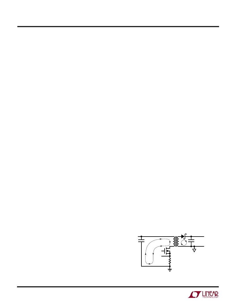
Keep the high current loops physically small in area. The
main loops are shown in Figure 6: the power switch loops
(A) and the rectifier loop (B). These loops can be kept small
by physically keeping the components close to one an-
other. In addition, connection traces should be kept wide
to lower resistance and inductances. Components should
be placed to minimize connecting paths. Careful attention
to ground connections must also be maintained. Be care-
ful that currents from different high current loops do not
get coupled into the ground paths of other loops. Using
singular points of connection for the grounds is the best
way to do this. The two major points of connection are the
bottom of the input decoupling capacitor and the bottom
of the output decoupling capacitor. Typically, the sense
resistor device PGND and device GND will tie to the bottom
of the input capacitor.
C
OUT
B
A
V
OUT
V
IN
GATE
CS
1738 F06
C
IN
Figure 6
相關(guān)PDF資料 |
PDF描述 |
|---|---|
| LT1761ES5-2 | 100mA, Low Noise, LDO Micropower Regulators in SOT-23 |
| LT1761ES5-2.5 | 100mA, Low Noise, LDO Micropower Regulators in SOT-23 |
| LT1761ES5-2.8 | 100mA, Low Noise, LDO Micropower Regulators in SOT-23 |
| LT1761ES5-3 | 100mA, Low Noise, LDO Micropower Regulators in SOT-23 |
| LT1761ES5-3.3 | 100mA, Low Noise, LDO Micropower Regulators in SOT-23 |
相關(guān)代理商/技術(shù)參數(shù) |
參數(shù)描述 |
|---|---|
| LT1738IG#PBF | 功能描述:IC REG CTRLR PWM CM 20-SSOP RoHS:是 類別:集成電路 (IC) >> PMIC - 穩(wěn)壓器 - DC DC 切換控制器 系列:- 標(biāo)準(zhǔn)包裝:4,500 系列:PowerWise® PWM 型:控制器 輸出數(shù):1 頻率 - 最大:1MHz 占空比:95% 電源電壓:2.8 V ~ 5.5 V 降壓:是 升壓:無 回掃:無 反相:無 倍增器:無 除法器:無 Cuk:無 隔離:無 工作溫度:-40°C ~ 125°C 封裝/外殼:6-WDFN 裸露焊盤 包裝:帶卷 (TR) 配用:LM1771EVAL-ND - BOARD EVALUATION LM1771 其它名稱:LM1771SSDX |
| LT1738IG#PBF | 制造商:Linear Technology 功能描述:ICSMPS CONTROLLERCURRENT-MODESSOP20P 制造商:Linear Technology 功能描述:IC,SMPS CONTROLLER,CURRENT-MODE,SSOP,20P |
| LT1738IG#TR | 功能描述:IC REG CTRLR PWM CM 20-SSOP RoHS:否 類別:集成電路 (IC) >> PMIC - 穩(wěn)壓器 - DC DC 切換控制器 系列:- 標(biāo)準(zhǔn)包裝:4,500 系列:PowerWise® PWM 型:控制器 輸出數(shù):1 頻率 - 最大:1MHz 占空比:95% 電源電壓:2.8 V ~ 5.5 V 降壓:是 升壓:無 回掃:無 反相:無 倍增器:無 除法器:無 Cuk:無 隔離:無 工作溫度:-40°C ~ 125°C 封裝/外殼:6-WDFN 裸露焊盤 包裝:帶卷 (TR) 配用:LM1771EVAL-ND - BOARD EVALUATION LM1771 其它名稱:LM1771SSDX |
| LT1738IG#TRPBF | 功能描述:IC REG CTRLR PWM CM 20-SSOP RoHS:是 類別:集成電路 (IC) >> PMIC - 穩(wěn)壓器 - DC DC 切換控制器 系列:- 標(biāo)準(zhǔn)包裝:4,500 系列:PowerWise® PWM 型:控制器 輸出數(shù):1 頻率 - 最大:1MHz 占空比:95% 電源電壓:2.8 V ~ 5.5 V 降壓:是 升壓:無 回掃:無 反相:無 倍增器:無 除法器:無 Cuk:無 隔離:無 工作溫度:-40°C ~ 125°C 封裝/外殼:6-WDFN 裸露焊盤 包裝:帶卷 (TR) 配用:LM1771EVAL-ND - BOARD EVALUATION LM1771 其它名稱:LM1771SSDX |
| LT1739 | 制造商:未知廠家 制造商全稱:未知廠家 功能描述:TRANSISTOR | BJT | NPN | 100V V(BR)CEO | 300MA I(C) | TO-39 |
發(fā)布緊急采購,3分鐘左右您將得到回復(fù)。