- 您現(xiàn)在的位置:買賣IC網(wǎng) > PDF目錄377705 > LT1510 (Linear Technology Corporation) Constant-Voltage/ Constant-Current Battery Charger PDF資料下載
參數(shù)資料
| 型號(hào): | LT1510 |
| 廠商: | Linear Technology Corporation |
| 英文描述: | Constant-Voltage/ Constant-Current Battery Charger |
| 中文描述: | 恒壓/恒流充電器 |
| 文件頁(yè)數(shù): | 4/16頁(yè) |
| 文件大小: | 339K |
| 代理商: | LT1510 |
第1頁(yè)第2頁(yè)第3頁(yè)當(dāng)前第4頁(yè)第5頁(yè)第6頁(yè)第7頁(yè)第8頁(yè)第9頁(yè)第10頁(yè)第11頁(yè)第12頁(yè)第13頁(yè)第14頁(yè)第15頁(yè)第16頁(yè)
4
LT1510/LT1510-5
ELECTRICAL CHARACTERISTICS
V
CC
= 16V, V
BAT
= 8V, V
MAX
(maximum operating V
CC
) = 28V, no load on any outputs, unless otherwise noted.
PARAMETER
Current Amplifier (CA2)
Transconductance
Maximum V
C
for Switch OFF
I
VC
Current (Out of Pin)
CONDITIONS
MIN
TYP
MAX
UNITS
V
C
= 1V, I
VC
=
±
1
μ
A
150
250
550
0.6
100
3
μ
mho
G
V
V
C
≥
0.6V
V
C
< 0.45V
μ
A
mA
Voltage Amplifier (VA), 16-Pin Only
Transconductance (Note 2)
Output Source Current, V
CC
= 10V
OVP Input Bias Current
Output Current from 100
μ
A to 500
μ
A
V
PROG
= V
OVP
= V
REF
+ 10mV
At 0.75mA VA Output Current
0.5
1.3
1.2
2.5
mho
mA
nA
G
50
150
The
G
denotes specifications which apply over the specified
temperature range.
Note 1:
Tested with Test Circuit 1.
Note 2:
Tested with Test Circuit 2.
Note 3:
Sense resistor R
S1
and package bond wires.
Note 4:
Applies to 16-pin only. 8-pin packages are guaranteed but not
tested at –40
°
C.
Note 5:
Current (
≈
700
μ
A) flows into the pins during normal operation and
also when an external shutdown signal on the V
C
pin is greater than 0.3V.
Current decreases to
≈
200
μ
A and flows out of the pins when external
shutdown holds the V
C
pin below 0.3V. Current drops to near zero when
input voltage collapses. See external Shutdown in Applications Information
section.
Note 6:
A linear interpolation can be used for reference voltage
specification between 0
°
C and –40
°
C.
Note 7:
Commercial grade device specifications are guaranteed over the
0
°
C to 70
°
C temperature range. In addition, commercial grade device
specifications are assured over the –40
°
C to 85
°
C temperature range by
design or correlation, but are not production tested.
Maximum allowable ambient temperature may be limited by power
dissipation. Parts may not necessarily be operated simultaneously at
maximum power dissipation and maximum ambient temperature.
Temperature rise calculations must be done as shown in the Applications
Information section to ensure that maximum junction temperature does
not exceed the 125
°
C limit. With high power dissipation, maximum
ambient temperature may be less than 70
°
C.
Note 8:
Industrial grade device specifications are guaranteed over the
–40
°
C to 85
°
C temperature range.
Note 9:
91% maximum duty cycle is guaranteed by design if V
BAT
or V
X
(see Figure 8 in Application Information) is kept between 3V and 5V.
Note 10:
V
BAT
= 4.2V.
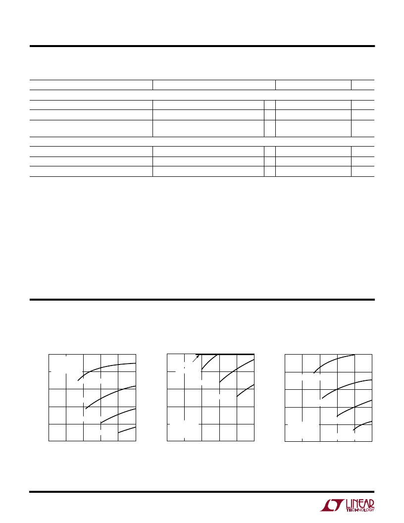
Thermally Limited Maximum
Charging Current, 8-Pin SO
INPUT VOLTAGE (V)
0
M
1.3
1.1
0.9
0.7
0.5
0.3
20
1510 G12
5
10
15
25
16V BATTERY
12V BATTERY
8V BATTERY
4V BATTERY
(
θ
JA
=125
°
C/W)
T
AMAX
=60
°
C
T
JMAX
=125
°
C
Thermally Limited Maximum
Charging Current, 16-Pin SO
INPUT VOLTAGE (V)
0
M
1.5
1.3
1.1
0.9
0.7
0.5
20
1510 G13
5
10
15
25
(
θ
JA
=50
°
C/W)
T
AMAX
=60
°
C
T
JMAX
=125
°
C
16V BATTERY
12V BATTERY
8V BATTERY
4V BATTERY
Thermally Limited Maximum
Charging Current, 16-Pin GN
INPUT VOLTAGE (V)
0
M
1.5
1.3
1.1
0.9
0.7
0.5
20
LT1510 TPC14
5
10
15
25
θ
JA
= 80
°
C/W
T
AMAX
= 60
°
C
T
JMAX
= 125
°
C
4V BATTERY
8V BATTERY
12V BATTERY
16V BATTERY
TYPICAL PERFOR
M
A
N
CE CHARACTERISTICS
相關(guān)PDF資料 |
PDF描述 |
|---|---|
| LT1510C | Constant-Voltage/ Constant-Current Battery Charger |
| LT1510I | Constant-Voltage/ Constant-Current Battery Charger |
| LT1510CN | Constant-Voltage/ Constant-Current Battery Charger |
| LT1510-5 | Constant-Voltage/ Constant-Current Battery Charger |
| LT1511CSW | Octal Bus Transceivers 20-SOIC 0 to 70 |
相關(guān)代理商/技術(shù)參數(shù) |
參數(shù)描述 |
|---|---|
| LT-1510-101-012 | 制造商:Carling Technologies 功能描述:LT-SERIES TOGGLE SWITCH - Bulk |
| LT-1510-110-012 | 功能描述:TOGGLE SW 15A 125VAC SOLDER LUG RoHS:是 類別:開關(guān) >> 撥動(dòng)開關(guān) 系列:LT 標(biāo)準(zhǔn)包裝:1 系列:A 電路:雙刀雙擲 開關(guān)功能:開-開-開 觸點(diǎn)額定電壓:6A @ 125VAC 觸動(dòng)器類型:扁平型 觸動(dòng)器長(zhǎng)度:11.38mm 發(fā)光:不發(fā)光 安裝類型:面板安裝 端接類型:焊片 軸襯螺紋:1/4-40 包裝:散裝 |
| LT-1510-110-024 | 制造商:Carling Technologies 功能描述:LT-SERIES TOGGLE SWITCH - Bulk |
| LT-1510-110-125 | 制造商:Carling Technologies 功能描述:LT-SERIES TOGGLE SWITCH - Bulk |
| LT-1510-115-125 | 制造商:Carling Technologies 功能描述:LT-SERIES TOGGLE SWITCH - Bulk |
發(fā)布緊急采購(gòu),3分鐘左右您將得到回復(fù)。