- 您現(xiàn)在的位置:買賣IC網(wǎng) > PDF目錄377704 > LT1468CS8 (LINEAR TECHNOLOGY CORP) 90MHz, 22V/us 16-Bit Accurate Operational Amplifier PDF資料下載
參數(shù)資料
| 型號: | LT1468CS8 |
| 廠商: | LINEAR TECHNOLOGY CORP |
| 元件分類: | 運動控制電子 |
| 英文描述: | 90MHz, 22V/us 16-Bit Accurate Operational Amplifier |
| 中文描述: | OP-AMP, 250 uV OFFSET-MAX, 88 MHz BAND WIDTH, PDSO8 |
| 封裝: | 0.150 INCH, PLASTIC, SOP-8 |
| 文件頁數(shù): | 4/12頁 |
| 文件大?。?/td> | 304K |
| 代理商: | LT1468CS8 |

4
LT1468
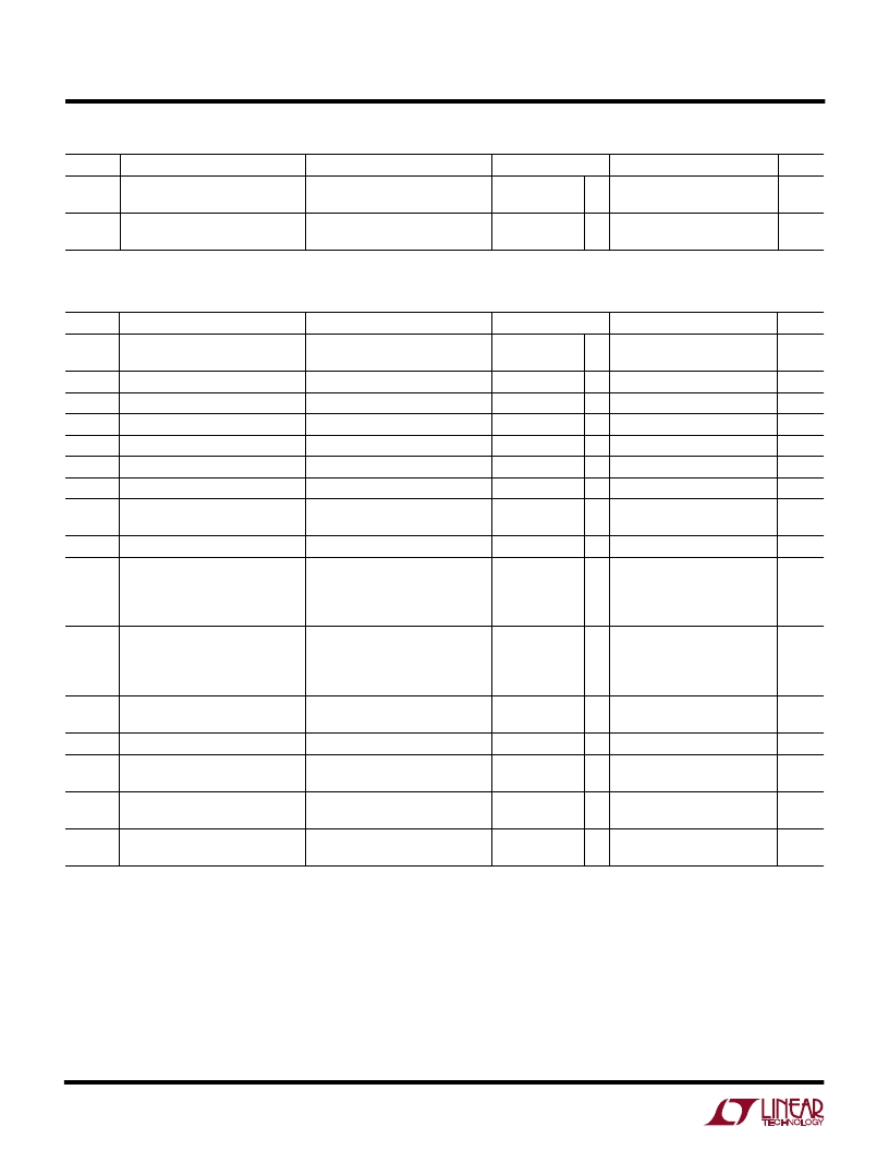
ELECTRICAL CHARACTERISTICS
0
°
C
≤
T
A
≤
70
°
C, V
CM
= 0V unless otherwise noted.
SYMBOL
V
OS
PARAMETER
Input Offset Voltage
CONDITIONS
V
SUPPLY
±
15V
±
5V
±
5V to
±
15V
±
5V to
±
15V
±
5V to
±
15V
±
5V to
±
15V
±
5V to
±
15V
±
5V to
±
15V
±
15V
±
5V
MIN
TYP
MAX
230
330
2.5
80
UNITS
G
G
μ
V
μ
V
Input V
OS
Drift
Input Offset Current
Input Offset Current Drift
Inverting Input Bias Current
Negative Input Current Drift
Noninverting Input Bias Current
Common Mode Rejection Ratio
(Note 7)
G
0.7
μ
V/
°
C
I
OS
G
nA
120
pA/
°
C
I
B–
G
±
30
nA
80
pA/
°
C
I
B+
CMRR
G
±
60
nA
dB
dB
dB
V
CM
=
±
12.5V
V
CM
=
±
2.5V
V
S
=
±
4.5V to
±
15V
V
OUT
=
±
12V, R
L
= 10k
V
OUT
=
±
10V, R
L
= 2k
V
OUT
=
±
2.5V, R
L
= 10k
V
OUT
=
±
2.5V, R
L
= 2k
R
L
= 10k, V
IN
=
±
1mV
R
L
= 2k, V
IN
=
±
1mV
R
L
= 10k, V
IN
=
±
1mV
R
L
= 2k, V
IN
=
±
1mV
V
OUT
=
±
12.5V
V
OUT
=
±
2.5V
V
OUT
= 0V, V
IN
=
±
0.2V
A
V
= –1, R
L
= 2k (Note 5)
G
G
92
92
96
300
150
300
150
±
12.8
±
12.6
±
2.8
±
2.6
±
7
±
7
±
12
9
6
45
40
PSRR
A
VOL
Power Supply Rejection Ratio
Large-Signal Voltage Gain
G
±
15V
±
15V
±
5V
±
5V
±
15V
±
15V
±
5V
±
5V
±
15V
±
5V
±
15V
±
15V
±
5V
±
15V
±
5V
±
15V
±
5V
G
G
G
G
V/mV
V/mV
V/mV
V/mV
V
OUT
Output Swing
G
G
G
G
V
V
V
V
I
OUT
Output Current
G
G
mA
mA
mA
V/
μ
s
V/
μ
s
MHz
MHz
mA
mA
I
SC
SR
Short-Circuit Current
Slew Rate
G
G
G
GBW
Gain Bandwidth
f = 100kHz, R
L
= 2k
G
G
I
S
Supply Current
G
G
7.0
6.8
–40
°
C
≤
T
A
≤
85
°
C, V
CM
= 0V unless otherwise noted (Note 4).
SYMBOL
GBW
PARAMETER
Gain Bandwidth
CONDITIONS
f = 100kHz, R
L
= 2k
V
SUPPLY
±
15V
±
5V
±
15V
±
5V
MIN
55
50
TYP
MAX
UNITS
MHz
MHz
mA
mA
G
G
I
S
Supply Current
G
G
6.5
6.3
The
G
denotes specifications that apply over the full operating
temperature range.
Note 1
: Absolute Maximum Ratings are those values beyond which the life
of a device may be impaired.
Note 2
: The inputs are protected by back-to-back diodes and two 100
series resistors. If the differential input voltage exceeds 0.7V, the input
current should be limited to 10mA. Input voltages outside the supplies will
be clamped by ESD protection devices and input currents should also be
limited to 10mA.
Note 3
: A heat sink may be required to keep the junction temperature
below absolute maximum when the output is shorted indefinitely.
Note 4
: The LT1468C is guaranteed to meet specified performance from
0
°
C to 70
°
C and is designed, characterized and expected to meet these
extended temperature limits, but is not tested at –40
°
C and at 85
°
C. The
LT1468I is guaranteed to meet the extended temperature limits.
Note 5
: Slew rate is measured between
±
8V on the output with
±
12V input
for
±
15V supplies and
±
2V on the output with
±
3V input for
±
5V supplies.
Note 6
: Full power bandwidth is calculated from the slew rate
measurement: FPBW = SR/2
π
V
P
Note 7
: This parameter is not 100% tested.
發(fā)布緊急采購,3分鐘左右您將得到回復(fù)。