- 您現(xiàn)在的位置:買賣IC網(wǎng) > PDF目錄377673 > LT1054 (Linear Technology Corporation) Switched-Capacitor Voltage Converter with Regulator(帶穩(wěn)壓器的開關(guān)電容電壓轉(zhuǎn)換器) PDF資料下載
參數(shù)資料
| 型號: | LT1054 |
| 廠商: | Linear Technology Corporation |
| 英文描述: | Switched-Capacitor Voltage Converter with Regulator(帶穩(wěn)壓器的開關(guān)電容電壓轉(zhuǎn)換器) |
| 中文描述: | 開關(guān)電容電壓轉(zhuǎn)換器穩(wěn)壓器(帶穩(wěn)壓器的開關(guān)電容電壓轉(zhuǎn)換器) |
| 文件頁數(shù): | 7/16頁 |
| 文件大小: | 281K |
| 代理商: | LT1054 |
7
LT1054/LT1054L
the oscillator frequency. During the time that C
IN
is charg-
ing, the peak supply current will be approximately equal to
2.2 times the output current. During the time that C
IN
is
delivering charge to C
OUT
the supply current drops to
approximately 0.2 times the output current. An input
supply bypass capacitor will supply part of the peak input
current drawn by the LT1054 and average out the current
drawn from the supply. A minimum input supply bypass
capacitor of 2
μ
F, preferably tantalum or some other low
ESR type is recommended. A larger capacitor may be
desirable in some cases, for example, when the actual input
supply is connected to the LT1054 through long leads, or
when the pulse current drawn by the LT1054 might affect
other circuitry through supply coupling.
PI
FU
CTIO
N
S
U
U
APPLICATIO
S I
FOR
ATIO
U
Theory of Operation
To understand the theory of operation of the LT1054, a
review of a basic switched-capacitor building block is
helpful.
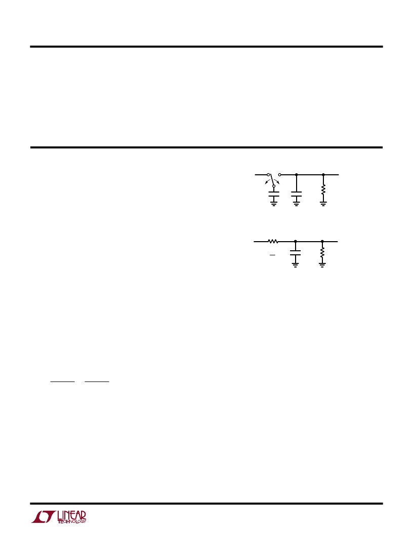
In Figure 3 when the switch is in the left position, capacitor
C1 will charge to voltage V1. The total charge on C1 will be
q1 = C1V1. The switch then moves to the right, discharging
C1 to voltage V2. After this discharge time the charge on C1
is q2 = C1V2. Note that charge has been transferred from
the source V1 to the output V2. The amount of charge
transferred is:
q = q1 – q2 = C1(V1 – V2)
If the switch is cycled f times per second, the charge
transfer per unit time (i.e., current) is:
I = (f)(
q) = (f)[C1(V1 – V2)]
To obtain an equivalent resistance for the switched-capaci-
tor network we can rewrite this equation in terms of voltage
and impedance equivalence:
W
U
U
I =
=
V1 – V2
(1/fC1)
V1 – V2
R
EQUIV
A new variable R
EQUIV
is defined such that R
EQUIV
= 1/fC1.
Thus the equivalent circuit for the switched-capacitor
network is as shown in Figure 4. The LT1054 has the same
switching action as the basic switched-capacitor building
block. Even though this simplification doesn’t include finite
switch on-resistance and output voltage ripple, it provides
an intuitive feel for how the device works.
These simplified circuits explain voltage loss as a function
of frequency (see Typical Performance Characteristics). As
frequency is decreased, the output impedance will eventu-
f
C1
C2
R
L
V2
LT1054 F03
V1
Figure 3. Switched-Capacitor Building Block
C2
R
L
R
EQUIV
R
EQUIV
=
V2
LT1054 F04
V1
1
fC1
Figure 4. Switched-Capacitor Equivalent Circuit
ally be dominated by the 1/fC1 term and voltage losses will
rise.
Note that losses also rise as frequency increases. This is
caused by internal switching losses which occur due to
some finite charge being lost on each switching cycle. This
charge loss per-unit-cycle, when multiplied by the switch-
ing frequency, becomes a current loss. At high frequency
this loss becomes significant and voltage losses again rise.
The oscillator of the LT1054 is designed to run in the
frequency band where voltage losses are at a minimum.
Regulation
T
he error amplifier of the LT1054 servos the drive to the
PNP switch to control the voltage across the input capaci-
tor (C
IN
) which in turn will determine the output voltage.
Using the reference and error amplifier of the LT1054, an
external resistive divider is all that is needed to set the
regulated output voltage. Figure 5 shows the basic regu-
lator configuration and the formula for calculating the
appropriate resistor values. R1 should be chosen to be
相關(guān)PDF資料 |
PDF描述 |
|---|---|
| LT1054L | Switched-Capacitor Voltage Converter with Regulator(帶穩(wěn)壓器的開關(guān)電容電壓轉(zhuǎn)換器) |
| LT1055 | Octal Buffers/Drivers With 3-State Outputs 20-PDIP 0 to 70 |
| LT1055S8 | Precision, High Speed, JFET Input Operational Amplifiers |
| LT1056CN8 | Precision, High Speed, JFET Input Operational Amplifiers |
| LT1055AM | Precision, High Speed, JFET Input Operational Amplifiers |
相關(guān)代理商/技術(shù)參數(shù) |
參數(shù)描述 |
|---|---|
| LT1054CDW | 功能描述:電荷泵 Bipolar Regulated V RoHS:否 制造商:Maxim Integrated 功能:Inverting, Step Up 輸出電壓:- 1.5 V to - 5.5 V, 3 V to 11 V 輸出電流:100 mA 電源電流:1 mA 最大工作溫度:+ 70 C 封裝 / 箱體:SOIC-8 Narrow 封裝:Tube |
| LT1054CDW | 制造商:Texas Instruments 功能描述: |
| LT1054CDWE4 | 功能描述:電荷泵 Switched-Capacitor Voltage Converter RoHS:否 制造商:Maxim Integrated 功能:Inverting, Step Up 輸出電壓:- 1.5 V to - 5.5 V, 3 V to 11 V 輸出電流:100 mA 電源電流:1 mA 最大工作溫度:+ 70 C 封裝 / 箱體:SOIC-8 Narrow 封裝:Tube |
| LT1054CDWG4 | 功能描述:電荷泵 Swed-Capacitor Vltg Converters RoHS:否 制造商:Maxim Integrated 功能:Inverting, Step Up 輸出電壓:- 1.5 V to - 5.5 V, 3 V to 11 V 輸出電流:100 mA 電源電流:1 mA 最大工作溫度:+ 70 C 封裝 / 箱體:SOIC-8 Narrow 封裝:Tube |
| LT1054CDWR | 功能描述:電荷泵 Bipolar Regulated V RoHS:否 制造商:Maxim Integrated 功能:Inverting, Step Up 輸出電壓:- 1.5 V to - 5.5 V, 3 V to 11 V 輸出電流:100 mA 電源電流:1 mA 最大工作溫度:+ 70 C 封裝 / 箱體:SOIC-8 Narrow 封裝:Tube |
發(fā)布緊急采購,3分鐘左右您將得到回復。