- 您現(xiàn)在的位置:買賣IC網(wǎng) > PDF目錄67757 > LSP3601SH (LITE-ON SEMICONDUCTOR CORP) SWITCHING CONTROLLER, 600 kHz SWITCHING FREQ-MAX, PDSO8 PDF資料下載
參數(shù)資料
| 型號: | LSP3601SH |
| 廠商: | LITE-ON SEMICONDUCTOR CORP |
| 元件分類: | 穩(wěn)壓器 |
| 英文描述: | SWITCHING CONTROLLER, 600 kHz SWITCHING FREQ-MAX, PDSO8 |
| 封裝: | SOP-8 |
| 文件頁數(shù): | 13/14頁 |
| 文件大小: | 425K |
| 代理商: | LSP3601SH |
Liteon Semiconductor Corporation
LSP3601
Step-Up DC/DC Controller
8/14
Rev1.3
Figure 12. Error Amplifier with Feedback resistance divider
Oscillator
The oscillator frequency can be set between 20 KHz and 500 KHz by connecting a resistor and a capacitor at OSC
pin of LSP3601 to ground. The oscillator frequency can be determined by using the graph shown in figure 9.
The oscillator output is a sawtooth wave with a minimum value of approximately 0.1V and a maximum value of
approximately 0.6V. The PWM comparator compares the oscillator voltage with error amplifier output voltage;
internal
DTC voltage (typ.0.6V) and soft start setting voltage. When the sawtooth wave is lower than the above three output
voltage, the output of LSP3601 is high (Turn on NPN transistor or NMOS).
Under voltage lockout (UVLO)
The under voltage lockout circuits turn the output off whenever the supply voltage drop too low (approximately
0.9V at 25 ℃) for proper operation .A hysterics voltage of 200 mV eliminates false triggering on noise and
chattering.
Soft Start / Short-circuit protection (S.S. / S.C.P.)
The soft start is function after power on, and the interval of the soft start time is determined by capacitor connected
to SCP pin (pin 2). When soft start function finished, the internal soft start voltage is setting high, but external SCP
pin is setting low in order to change to short circuit detection / protection function.
The time of soft start is following expression:
TSS=0.35*C[μF]
The short circuit protection is functional due to a heavy loading drop and output of error amplifier (COMP pin) is
maintain a VPOS (typ.0.87V), the capacitor is charged until SCP threshold voltage (typ.0.8V), then LSP3601 output is
disable (internal pull-low ) and the capacitor is discharged to low .
The time of short circuit protection is following expression:
TSCP=0.8*C[μF]
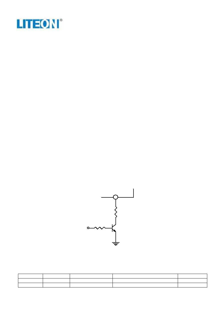
Output transistor
The LSP3601 has a totem-pole transistor with a 40 mA source/sink current rating to drive an external NPN transistor
or NMOS transistor directly. The driving current capability depends on a resistor R that is connected to BR/CTL pin
(pin4) of LSP3601. (see fig.13)
BR/CTL
R
Control
Q1
LSP3601
4
Figure13. Output transistor driving control circuit
BR/CTL pin can also use to control the output of LSP3601 for disable or enable function of system.
Control Pin
Q1
BR/CTL Pin
Output Transistor Function
Mode
Low
Off
Open
Disable
Stand-by
High
On
Bias Current
Enable
Operation
相關(guān)PDF資料 |
PDF描述 |
|---|---|
| LSP5502SAC | SWITCHING REGULATOR, 470 kHz SWITCHING FREQ-MAX, PDSO8 |
| LSP5502SC | SWITCHING REGULATOR, 470 kHz SWITCHING FREQ-MAX, PDSO8 |
| LT1054CN | SWITCHED CAPACITOR REGULATOR, 25 kHz SWITCHING FREQ-MAX, PDIP8 |
| LT1054MJ | SWITCHED CAPACITOR REGULATOR, 25 kHz SWITCHING FREQ-MAX, CDIP8 |
| LT1054CJ | SWITCHED CAPACITOR REGULATOR, 25 kHz SWITCHING FREQ-MAX, CDIP8 |
相關(guān)代理商/技術(shù)參數(shù) |
參數(shù)描述 |
|---|---|
| LSP380 | 制造商:INFINEON 制造商全稱:Infineon Technologies AG 功能描述:Plane 3 mm (T1) LED, Non Diffused |
| LSP380-MP | 制造商:INFINEON 制造商全稱:Infineon Technologies AG 功能描述:Plane 3 mm (T1) LED, Non Diffused |
| LSP380-N | 制造商:INFINEON 制造商全稱:Infineon Technologies AG 功能描述:Plane 3 mm (T1) LED, Non Diffused |
| LSP380-NQ | 制造商:INFINEON 制造商全稱:Infineon Technologies AG 功能描述:Plane 3 mm (T1) LED, Non Diffused |
| LSP380-P | 制造商:INFINEON 制造商全稱:Infineon Technologies AG 功能描述:Plane 3 mm (T1) LED, Non Diffused |
發(fā)布緊急采購,3分鐘左右您將得到回復(fù)。