- 您現(xiàn)在的位置:買賣IC網(wǎng) > PDF目錄358940 > LR38616 (Sharp Corporation) Timing Generator IC for 2 140 k-pixel CCDs PDF資料下載
參數(shù)資料
| 型號(hào): | LR38616 |
| 廠商: | Sharp Corporation |
| 英文描述: | Timing Generator IC for 2 140 k-pixel CCDs |
| 中文描述: | 時(shí)序發(fā)生器集成電路2 140的k -像素CCD |
| 文件頁數(shù): | 3/9頁 |
| 文件大小: | 64K |
| 代理商: | LR38616 |
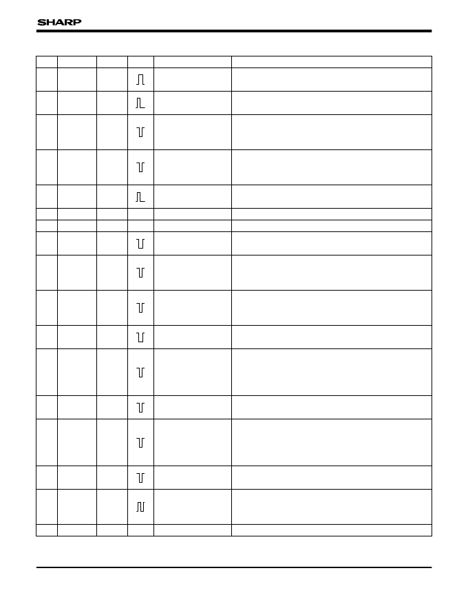
3
LR38616
PIN NO.
SYMBOL
I/O
POLARITY
PIN NAME
Control pulse output
for OFD voltage
Vertical transfer
pulse output 1
DESCRIPTION
1
OFDC
O3
A pulse to control OFD voltage.
2
V
1X
O3
A vertical transfer pulse for CCD.
Connect to V
1X
pin of vertical driver IC.
A pulse that transfers the charge of the photo-diode to
the vertical shift register.
Connect to VH
1AX
pin of vertical driver IC.
A pulse that transfers the charge of the photo-diode to
the vertical shift register.
Connect to VH
1BX
pin of vertical driver IC.
A vertical transfer pulse for CCD.
Connect to V
2X
pin of vertical driver IC.
Supply of +3.3 V power.
A grounding pin.
A vertical transfer pulse for CCD.
Connect to V
3X
pin of vertical driver IC.
3
VH
1AX
O3
Readout pulse
output 1A
4
VH
1BX
O3
Readout pulse
output 1B
5
V
2X
O3
Vertical transfer
pulse output 2
Power supply
Ground
Vertical transfer
pulse output 3
6
7
V
DD3
GND
–
–
–
9
VH
3AX
O3
Readout pulse
output 3A
A pulse that transfers the charge of the photo-diode to
the vertical shift register.
Connect to VH
3AX
pin of vertical driver IC.
A pulse that transfers the charge of the photo-diode to
the vertical shift register.
Connect to VH
3BX
pin of vertical driver IC.
A vertical transfer pulse for CCD.
Connect to V
4X
pin of vertical driver IC.
A pulse that sweeps the charge of the photo-diode for
the electronic shutter. Connect to OFD pin of CCD
through the vertical driver IC and DC offset circuit.
Held at H level at normal mode.
A pulse that corresponds to the cease period of the
horizontal transfer pulse.
A pulse to clamp the optical black signal.
This pulse stays high during the absence of
effective pixels within the vertical blanking or the period
of sweep-out signal.
A pulse to clamp the dummy outputs of CCD signal.
This pulse stays high during the sweep-out period.
An output pin for AD converter.
The output phase of ADCK is selected by serial data
step by 90.
A grounding pin.
8
V
3X
O3
Readout pulse
output 3B
O3
VH
3BX
10
11
V
4X
O3
Vertical transfer
pulse output 4
OFD pulse output
O3
OFDX
12
13
PBLK
O3
Pre-blanking pulse
output
Optical black clamp
pulse output
O3
BCPX
14
15
CLPX
O3
Clamp pulse output
AD clock output
O6MA3
ADCK
16
17
GND
–
Ground
–
–
PIN DESCRIPTION
相關(guān)PDF資料 |
PDF描述 |
|---|---|
| LR38620 | Timing Generator IC for 4200 k-pixwl CCD |
| LR38630 | Digital Signal Processor for CIF CMOS Image Cameras |
| LR38666Y | CMOS digital signal processor |
| LR4-260 | PolySwitch PTC Devices Overcurrent Protection Device |
| LR4089B | Tone Dialer LSI |
相關(guān)代理商/技術(shù)參數(shù) |
參數(shù)描述 |
|---|---|
| LR38617 | 制造商:Sharp Microelectronics Corporation 功能描述:TIMING GENERATOR 48PQFP - Bulk |
| LR38620 | 制造商:SHARP 制造商全稱:Sharp Electrionic Components 功能描述:Timing Generator IC for 4200 k-pixwl CCD |
| LR38627 | 制造商:SHARP 制造商全稱:Sharp Electrionic Components 功能描述:Digital SIgnal Processing LSI for CCD |
| LR38630 | 制造商:SHARP 制造商全稱:Sharp Electrionic Components 功能描述:Digital Signal Processor for CIF CMOS Image Cameras |
| LR38637 | 制造商:SHARP 制造商全稱:Sharp Electrionic Components 功能描述:Digital Signal Processor For VGA/CIF CMOS Image Sensors |
發(fā)布緊急采購,3分鐘左右您將得到回復(fù)。