- 您現(xiàn)在的位置:買賣IC網(wǎng) > PDF目錄367583 > LP395 PDF資料下載
參數(shù)資料
| 型號(hào): | LP395 |
| 文件頁(yè)數(shù): | 2/5頁(yè) |
| 文件大小: | 130K |
| 代理商: | LP395 |
Absolute Maximum Ratings
(Note 1)
Collector to Emitter Voltage
Collector to Base Voltage
Base to Emitter Voltage (Forward)
Base to Emitter Voltage (Reverse)
Base to Emitter Current (Reverse)
36V
36V
36V
10V
20 mA
Collector Current Limit
Power Dissipation
Operating Temperature Range
Storage Temperature Range
Lead Temp. (Soldering, 10 seconds)
Internally Limited
Internally Limited
40C to +125C
65C to +150C
260C
Electrical Characteristics
Tested
Limit
(Note 3)
36
Design
Limit
(Note 4)
36
(Note 2)
20
50
100
2.5
0.60
2.10
36
Units
(Limit)
Symbol
Parameter
Conditions
Typical
V
CE
Collector to Emitter
Operating Voltage
Collector Current Limit
(Note 5)
0.5 mA
≤
I
C
≤
100 mA
V(Max)
I
CL
V
BE
= 2V, V
CE
= 36V
V
BE
= 2V, V
CE
= 15V
V
BE
= 2V, 2V
≤
V
CE
≤
6V
0
≤
I
C
≤
100 mA
V
BE
= 0V, 0
≤
V
CE
≤
36V
V
BE
= 2V, I
C
= 100 mA
0
≤
V
CE
≤
36V, I
B
= 2 μA
45
90
130
0.3
0.24
1.82
25
60
100
2.0
0.50
2.00
36
mA(Min)
mA(Min)
mA(Min)
μA(Max)
mA(Max)
V(Max)
V(Min)
I
B
I
Q
V
CE(SAT)
BV
BE
Base Current
Quiescent Current
Saturation Voltage
Base to Emitter Break-
down Voltage (Note 5)
Base to Emitter Voltage
(Note 6)
Switching Time
V
BE
I
C
= 5 mA
I
C
= 100 mA (Note 5)
V
CE
= 20V, R
L
= 200
V
BE
= 0V, +2V, 0V
0.4" leads soldered to
printed circuit board
0.125" leads soldered to
printed circuit board
0.69
1.02
2
0.79
0.90
1.40
V(Max)
V (Max)
μs
t
S
θ
JA
Thermal Resistance
Junction to Ambient
150
180
C/W
(Max)
C/W
(Max)
130
160
Note 1:
Absolute Maximum Ratings indicate limits beyond which damage to the device may occur. Operating Ratings indicate conditions for which the device is func-
tional, but do not guarantee specific performance limits.
Note 2:
Parameters identified with
boldface type
apply at temp. extremes. All other numbers, unless noted apply at +25C.
Note 3:
Guaranteed and 100% production tested.
Note 4:
Guaranteed (but not 100% production tested) over the operating temperature and supply voltage ranges. These limits are not used to calculate outgoing
quality levels.
Note 5:
These numbers apply for pulse testing with a low duty cycle.
Note 6:
Base positive with respect to emitter.
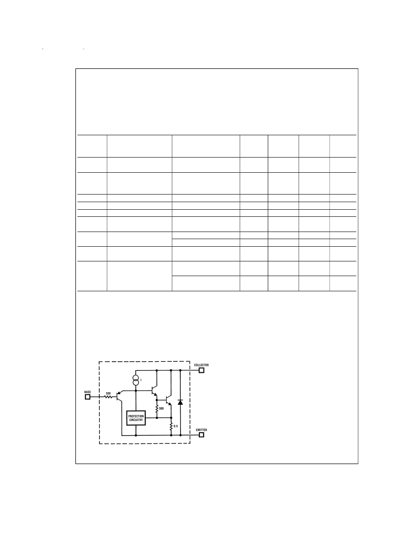
Simplified Circuit
Applications Information
One failure mode incandescent lamps may experience is
one in which the filament resistance drops to a very low
value before it actually blows out. This is especially rough on
most solid-state lamp drivers and in most cases a lamp fail-
ure of this type will also cause the lamp driver to fail. Be-
cause of its high gain and blowout-proof design, the LP395 is
an ideal candidate for reliably driving small incandescent
lamps. Additionally, the current limiting characteristics of the
LP395 are advantageous as it serves to limit the cold fila-
ment inrush current, thus increasing lamp life.
DS005525-5
www.national.com
2
相關(guān)PDF資料 |
PDF描述 |
|---|---|
| LP395Z | IC-POWER TRANSISTOR |
| LP3961 | |
| LP3961EMP-1.8 | THREE-TERMINAL POSITIVE FIXED VOLTAGE REGULATORS |
| LP3961EMP-3.3 | THREE-TERMINAL POSITIVE FIXED VOLTAGE REGULATORS |
| LP3961EMPX-1.8 | THREE-TERMINAL POSITIVE FIXED VOLTAGE REGULATORS |
相關(guān)代理商/技術(shù)參數(shù) |
參數(shù)描述 |
|---|---|
| LP3950 | 制造商:NSC 制造商全稱:National Semiconductor 功能描述:Color LED Driver with Audio Synchronizer |
| LP3950SL | 制造商:Texas Instruments 功能描述:LED DRIVER COLOUR POWERWISE LLP32 |
| LP3950SL/CSP1 | 制造商:Rochester Electronics LLC 功能描述: 制造商:Texas Instruments 功能描述: |
| LP3950SL/NOPB | 功能描述:LED照明驅(qū)動(dòng)器 RoHS:否 制造商:STMicroelectronics 輸入電壓:11.5 V to 23 V 工作頻率: 最大電源電流:1.7 mA 輸出電流: 最大工作溫度: 安裝風(fēng)格:SMD/SMT 封裝 / 箱體:SO-16N |
| LP3950SLX | 制造商:NSC 制造商全稱:National Semiconductor 功能描述:Color LED Driver with Audio Synchronizer |
發(fā)布緊急采購(gòu),3分鐘左右您將得到回復(fù)。