- 您現(xiàn)在的位置:買賣IC網(wǎng) > PDF目錄358906 > LP2952IN-3.3 (NATIONAL SEMICONDUCTOR CORP) Adjustable Micropower Low-Dropout Voltage Regulators PDF資料下載
參數(shù)資料
| 型號: | LP2952IN-3.3 |
| 廠商: | NATIONAL SEMICONDUCTOR CORP |
| 元件分類: | 基準(zhǔn)電壓源/電流源 |
| 英文描述: | Adjustable Micropower Low-Dropout Voltage Regulators |
| 中文描述: | FIXED/ADJUSTABLE POSITIVE LDO REGULATOR, 0.8 V DROPOUT, PDIP14 |
| 封裝: | PLASTIC, DIP-14 |
| 文件頁數(shù): | 3/22頁 |
| 文件大小: | 1050K |
| 代理商: | LP2952IN-3.3 |

Absolute Maximum Ratings
(Note 1)
If Military/Aerospace specified devices are required,
please contact the National Semiconductor Sales Office/
Distributors for availability and specifications.
Storage Temperature Range
65C
≤
T
A
≤
+150C
Operating Temperature Range
LP2952I, LP2953I, LP2952AI,
LP2953AI, LP2952I-3.3,
LP2953I-3.3, LP2952AI-3.3,
LP2953AI-3.3
LP2953AM
40C
≤
T
J
≤
+125C
55C
≤
T
A
≤
+125C
260C
Lead Temp. (Soldering, 5 seconds)
Power Dissipation (Note 2)
Internally Limited
Maximum Junction Temperature
LP2952I, LP2953I, LP2952AI,
LP2953AI, LP2952I-3.3,
LP2953I-3.3, LP2952AI-3.3,
LP2953AI-3.3
LP2953AM
Input Supply Voltage
Feedback Input Voltage (Note 3)
Comparator Input Voltage (Note 4)
Shutdown Input Voltage (Note 4)
Comparator Output Voltage (Note
4)
ESD Rating (Note 15)
+125C
+150C
20V to +30V
0.3V to +5V
0.3V to +30V
0.3V to +30V
0.3V to +30V
2 kV
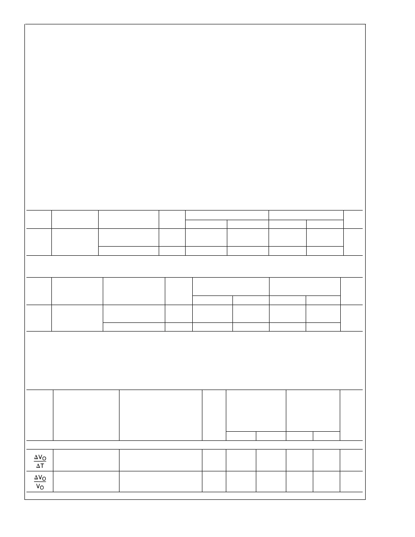
Electrical Characteristics
operating temperature range. Limits are guaranteed by production testing or correlation techniques using standard Statistical
Quality Control (SQC) methods. Unless otherwise specified: V
IN
= V
O
(NOM) + 1V, I
L
= 1 mA, C
L
= 2.2 μF for 5V parts and
4.7μF for 3.3V parts. Feedback pin is tied to V Tap pin, Output pin is tied to Output Sense pin.
3.3V Versions
Limits in standard typeface are for T
J
= 25C,
bold typeface
applies over the full
Symbol
Parameter
Conditions
Typical
LP2952AI-3.3, LP2953AI-3.3
Min
3.284
3.260
3.254
LP2952I-3.3, LP2953I-3.3
Min
3.267
3.234
3.221
Units
Max
3.317
3.340
3.346
Max
3.333
3.366
3.379
V
O
Output Voltage
3.3
V
1 mA
≤
I
L
≤
250 mA
3.3
5V Versions
Symbol
Parameter
Conditions
Typical
LP2952AI, LP2953AI,
LP2953AM
(Note 17)
Min
4.975
4.940
4.930
LP2952I, LP2953I
Units
Max
5.025
5.060
5.070
Min
4.950
4.900
4.880
Max
5.050
5.100
5.120
V
O
Output Voltage
5.0
V
1 mA
≤
I
L
≤
250 mA
5.0
All Voltage Options
Electrical Characteristics
Limits in standard typeface are for T
J
= 25C,
bold typeface
applies over the full operating temperature range. Limits are guar-
anteed by production testing or correlation techniques using standard Statistical Quality Control (SQC) methods. Unless other-
wise specified: V
= V
(NOM) + 1V, I
= 1 mA, C
L
= 2.2 μF for 5V parts and 4.7μF for 3.3V parts. Feedback pin is tied to V
Tap pin, Output pin is tied to Output Sense pin.
Symbol
Parameter
Conditions
Typical LP2952AI, LP2953AI,
LP2952AI-3.3,
LP2953AI-3.3,
LP2953AM
(Notes 16, 17)
Min
LP2952I, LP2953I,
LP2952I-3.3,
LP2953I-3.3
Units
Max
Min
Max
REGULATOR
Output Voltage Temp.
Coefficient
(Note 5)
20
100
150
ppm/C
Output Voltage Line
Regulation
V
IN
= V
O
(NOM) + 1V to 30V
0.03
0.1
0.2
%
0.2
0.4
L
www.national.com
3
相關(guān)PDF資料 |
PDF描述 |
|---|---|
| LP2952AIM | Adjustable Micropower Low-Dropout Voltage Regulators |
| LP2952IN | Adjustable Micropower Low-Dropout Voltage Regulators |
| LP2952AI-3.3 | Adjustable Micropower Low-Dropout Voltage Regulators |
| LP2952AI | Adjustable Micropower Low-Dropout Voltage Regulators |
| LP2952A | Adjustable Micropower Low-Dropout Voltage Regulators |
相關(guān)代理商/技術(shù)參數(shù) |
參數(shù)描述 |
|---|---|
| LP2953 | 制造商:NSC 制造商全稱:National Semiconductor 功能描述:Adjustable Micropower Low-Dropout Voltage Regulators |
| LP2953 MDS | 制造商:Texas Instruments 功能描述:- Gel-pak, waffle pack, wafer, diced wafer on film |
| LP2953A | 制造商:NSC 制造商全稱:National Semiconductor 功能描述:Adjustable Micropower Low-Dropout Voltage Regulators |
| LP2953AI | 制造商:NSC 制造商全稱:National Semiconductor 功能描述:Adjustable Micropower Low-Dropout Voltage Regulators |
| LP2953AI-3.3 | 制造商:NSC 制造商全稱:National Semiconductor 功能描述:Adjustable Micropower Low-Dropout Voltage Regulators |
發(fā)布緊急采購,3分鐘左右您將得到回復(fù)。