- 您現(xiàn)在的位置:買賣IC網(wǎng) > PDF目錄358905 > LP2950CT-3.3 100 mA Low Dropout Voltage Regulators PDF資料下載
參數(shù)資料
| 型號: | LP2950CT-3.3 |
| 元件分類: | 基準電壓源/電流源 |
| 英文描述: | 100 mA Low Dropout Voltage Regulators |
| 中文描述: | 一〇 〇毫安低壓差穩(wěn)壓器 |
| 文件頁數(shù): | 3/14頁 |
| 文件大小: | 142K |
| 代理商: | LP2950CT-3.3 |

Advanced Monolithic Systems, Inc.
6680B Sierra Lane, Dublin, CA 94568 Phone (925) 556-9090 Fax (925) 556-9140
LP2950/LP2951
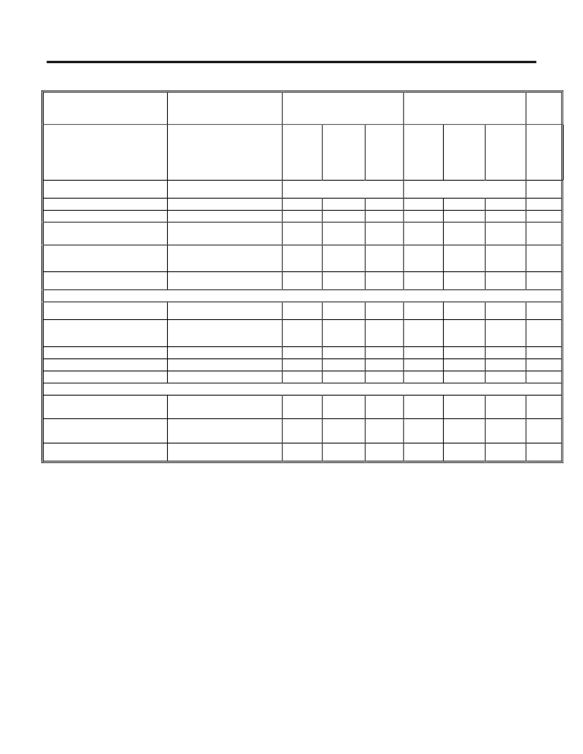
ELECTRICAL CHARACTERISTICS
(Note 2) (Continued)
PARAMETER
CONDITIONS
(Note 2)
CL = 1
μ
F
CL = 200
μ
F
CL = 13.3
μ
F
(Bypass = 0.01
μ
F pins 7 to
1(LP2951))
LP2950AC
LP2951AC
Min. Typ. Max.
LP2950C
LP2951C
Min. Typ. Max.
Units
Output Noise,
10Hz to 100KHz
430
160
100
430
160
100
μ
V rms
μ
V rms
μ
V rms
8-Pin Versions only
LP2951AC
LP2951C
Reference Voltage
Reference Voltage
1.22
1.19
1.235
1.25
1.27
1.21
1.185
1.235
1.26
1.285
V
V
Over Temperature (Note 7)
Feedback Pin Bias Current
40
60
40
60
nA
Reference Voltage Temperature
Coefficient
( Note 12 )
20
50
ppm/°C
Feedback Pin Bias Current
Temperature Coefficient
Error Comparator
0.1
0.1
nA/°C
Output Leakage Current
V
OH
= 30V
0.01
1
0.01
1
μ
A
Output Low Voltage
Vin = 4.5V
IOL = 400
μ
A
(Note 6)
(Note 6)
(Note 6)
150
250
150
250
mV
Upper Threshold Voltage
Lower Threshold Voltage
Hysteresis
Shutdown Input
40
60
75
15
40
60
75
15
mV
mV
mV
95
95
Input logic Voltage
Low (Regulator ON)
High (Regulator OFF)
2
1.3
0.7
2
1.3
0.7
V
V
μ
A
μ
A
Shutdown Pin Input Current
(Note 3)
Vs = 2.4V
Vs = 30V
30
450
50
600
30
450
50
600
Regulator Output Current in
Shutdown (Note 3)
(Note 11)
3
10
3
10
μ
A
Note 1:
Absolute Maximum Ratings are limits beyond which damage to the device may occur. Operating Ratings are conditions under which operation of the
device is guaranteed. Operating Ratings do not imply guaranteed performance limits. For guaranteed performance limits and associated test conditions, see the
Electrical Characteristics tables.
Note 2:
Unless otherwise specified all limits guaranteed for V
IN
= (
V
ONOM
+1)V, I
L
= 100
μ
A and C
L
= 1
μ
F for 5V versions and 2.2
μ
F for 3V and 3.3V versions.
Limits appearing in
boldface
type apply over the entire junction temperature range for operation. Limits appearing in normal type apply for T
A
= T
J
= 25
°
C
Additional conditions for the 8-pin versions are FEEDBACK tied to V
TAP
, OUTPUT tied to SENSE and V
SHUTDOWN
≤
0.8V.
Note 3:
Guaranteed and 100% production tested.
Note 4:
Guaranteed but not 100% production tested. These limits are not used to calculate outgoing AQL levels.
Note 5:
Dropout voltage is defined as the input to output differential at which the output voltage drops 100 mV below its nominal value measured at 1V differential.
At very low values of programmed output voltage, the minimum input supply voltage of 2V ( 2.3V over temperature) must be taken into account.
Note 6:
Comparator thresholds are expressed in terms of a voltage differential at the feedback terminal below the nominal reference voltage measured at
V
IN
= (
V
ONOM
+1)V. To express these thresholds in terms of output voltage change, multiply by the error amplifier gain = Vout/Vref = (R1 + R2)/R2. For example,
at a programmed output voltage of 5V, the error output is guaranteed to go low when the output drops by 95 mV x 5V/1.235 = 384 mV. Thresholds remain constant
as a percent of V
out
as V
out
is varied, with the dropout warning occurring at typically 5% below nominal, 7.5% guaranteed.
Note 7:
V
ref
≤
V
out
≤
(V
in
- 1V), 2.3
≤
V
in
≤
30V, 100
μ
A
≤
I
L
≤
100 mA, T
J
≤
T
JMAX
.
Note 8:
The junction-to-ambient thermal resistance are as follows:180
°
C/W and 160
°
C/W for the TO-92 (N) package with 0.40 inch and 0.25 inch leads to the
printed circuit board (PCB) respectively, 105
°
C/W for the molded plastic DIP (P) and 160
°
C/W for the molded plastic SO-8 (S). The above thermal resistances for
the N, S and P packages apply when the package is soldered directly to the PCB.
Note 9:
May exceed input supply voltage.
Note 10:
When used in dual-supply systems where the output terminal sees loads returned to a negative supply, the output voltage should be diode-clamped to
ground.
Note 11:
V
shutdown
≥
2V, V
in
≤
30V, V
out
=0, Feedback pin tied to 5V
TAP
.
Note 12:
Output or reference voltage temperature coefficients defined as the worst case voltage change divided by the total temperature range.
相關PDF資料 |
PDF描述 |
|---|---|
| LP2950CT-5.0 | 100 mA Low Dropout Voltage Regulators |
| LP2950CS-3.3 | 100 mA Low Dropout Voltage Regulators |
| LP2950CS-3.0 | 100 mA Low Dropout Voltage Regulators |
| LP2950AS-5.0 | 100 mA Low Dropout Voltage Regulators |
| LP2950AS-3.3 | 100 mA Low Dropout Voltage Regulators |
相關代理商/技術參數(shù) |
參數(shù)描述 |
|---|---|
| LP2950CT-5.0 | 制造商:SIPEX 制造商全稱:Sipex Corporation 功能描述:100 mA Low Dropout Voltage Regulators |
| LP2950CZ | 制造商:未知廠家 制造商全稱:未知廠家 功能描述:Micropower Voltage Regulators(251.36 k) |
| LP2950CZ3.0 | 制造商:ONSEMI 制造商全稱:ON Semiconductor 功能描述:100 mA, Low Power Low Dropout Voltage Regulator |
| LP2950CZ-3.0 | 功能描述:低壓差穩(wěn)壓器 - LDO RoHS:否 制造商:Texas Instruments 最大輸入電壓:36 V 輸出電壓:1.4 V to 20.5 V 回動電壓(最大值):307 mV 輸出電流:1 A 負載調節(jié):0.3 % 輸出端數(shù)量: 輸出類型:Fixed 最大工作溫度:+ 125 C 安裝風格:SMD/SMT 封裝 / 箱體:VQFN-20 |
| LP2950CZ-3.0 NOPB | 制造商:National Semiconductor 功能描述:LDO Regulator Pos 3V 0.1A 3-Pin TO-92 Box |
發(fā)布緊急采購,3分鐘左右您將得到回復。