- 您現(xiàn)在的位置:買賣IC網(wǎng) > PDF目錄98001 > LOG104AIDRE4 (TEXAS INSTRUMENTS INC) LOG OR ANTILOG AMPLIFIER, 0.01 MHz BAND WIDTH, PDSO8 PDF資料下載
參數(shù)資料
| 型號: | LOG104AIDRE4 |
| 廠商: | TEXAS INSTRUMENTS INC |
| 元件分類: | 模擬運算功能 |
| 英文描述: | LOG OR ANTILOG AMPLIFIER, 0.01 MHz BAND WIDTH, PDSO8 |
| 封裝: | ROHS COMPLIANT, PLASTIC, MS-012AA, SOIC-8 |
| 文件頁數(shù): | 6/13頁 |
| 文件大?。?/td> | 244K |
| 代理商: | LOG104AIDRE4 |
www.ti.com
LOG104
2
SBOS243C
ELECTROSTATIC
DISCHARGE SENSITIVITY
This integrated circuit can be damaged by ESD. Texas Instru-
ments recommends that all integrated circuits be handled with
appropriate precautions. Failure to observe proper handling
and installation procedures can cause damage.
ESD damage can range from subtle performance degrada-
tion to complete device failure. Precision integrated circuits
may be more susceptible to damage because very small
parametric changes could cause the device not to meet its
published specifications.
ABSOLUTE MAXIMUM RATINGS(1)
Supply Voltage, V+ to V– .................................................................... 36V
Input Voltage ....................................................... V– (–0.5) to V+ (+0.5V)
Input Current ...................................................................................
±10mA
Output Short-Circuit(2) .............................................................. Continuous
Operating Temperature .................................................... –40
°C to +85°C
Storage Temperature ..................................................... –55
°C to +125°C
Junction Temperature .................................................................... +150
°C
Lead Temperature (soldering, 10s) ............................................... +300
°C
NOTES: (1) Stresses above these ratings may cause permanent damage.
Exposure to absolute maximum conditions for extended periods may degrade
device reliability. (2) Short-circuit to ground.
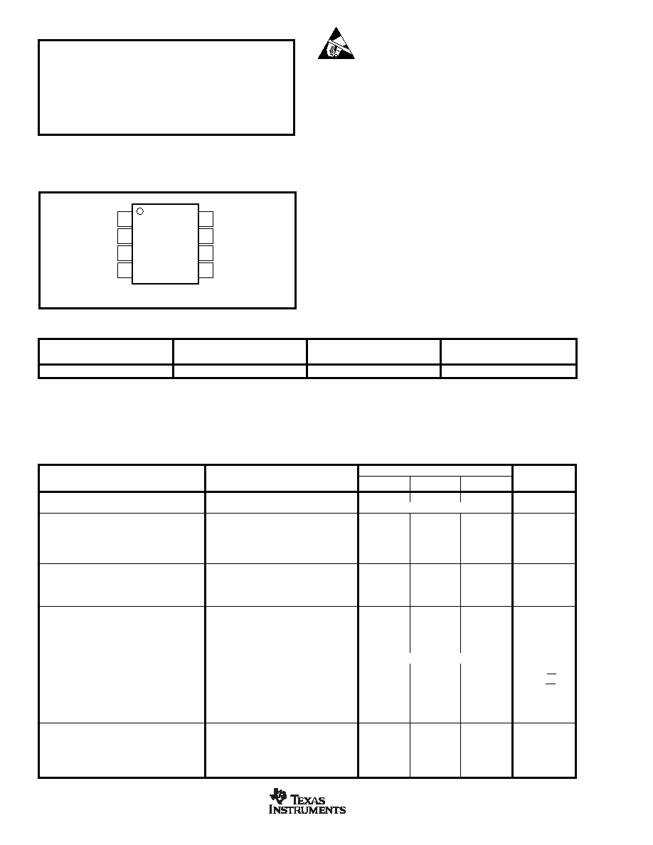
PIN DESCRIPTION
ELECTRICAL CHARACTERISTICS
Boldface limits apply over the specified temperature range, TA = –5°C to +75°C.
At TA = +25°C, VS = ±5V, ROUT = 10k, unless otherwise noted.
Top View
SO
I
2
NC
GND
V–
NC = No Internal Connection
LOG104
I
1
NC
V
OUT
V+
8
7
6
5
1
2
3
4
LOG104AID
PARAMETER
CONDITION
MIN
TYP
MAX
UNITS
CORE LOG FUNCTION
IIN /VOUT Equation
VO = (0.5V)log (I1/I2)V
LOG CONFORMITY ERROR(1)
Initial
1nA to 100
A (5 decades)
0.01
0.2
%
100pA to 3.5mA (7.5 decades)
0.06
%
over Temperature
1nA to 100
A (5 decades)
0.0001
%/
°C
100pA to 3.5mA (7.5 decades)(2)
0.0005
%/
°C
GAIN(3)
Initial Value
1nA to 100
A
0.5
V/decade
Gain Error
1nA to 100
A
0.15
±1%
vs Temperature
TMIN to TMAX
0.003
0.01
%/
°C
INPUT, A1 and A2
Offset Voltage
±0.3
±1.5
mV
vs Temperature
TMIN to TMAX
±2
V/
°C
vs Power Supply (PSRR)
VS = ±4.5V to ±18V
5
50
V/V
Input Bias Current
±5pA
vs Temperature
TMIN to TMAX
Doubles Every 10
°C
Voltage Noise
f = 10Hz to 10kHz
3
Vrms
f = 1kHz
30
nV/
√Hz
Current Noise
f = 1kHz
4
fA/
√Hz
Common-Mode Voltage Range (Positive)
(V+) – 2
(V+) – 1.5
V
(Negative)
(V–) + 2
(V–) + 1.2
V
Common-Mode Rejection Ratio (CMRR)
105
dB
OUTPUT, A2 (VOUT)
Output Offset, VOSO, Initial
±3
±15
mV
vs Temperature
TMIN to TMAX
±2
V/°C
Full-Scale Output (FSO)
VS = ±5V
(V–) + 1.2
(V+) – 1.5
V
Short-Circuit Current
±18
mA
PACKAGE
PRODUCT
PACKAGE-LEAD
DESIGNATOR
MARKING
LOG104AID
SO -8
D
LOG104
NOTES: (1) For the most current package and ordering information, see the Package Option Addendum at the end of this document, or see the TI website at
www.ti.com.
PACKAGE/ORDERING INFORMATION(1)
相關(guān)PDF資料 |
PDF描述 |
|---|---|
| LPR4150AL | SPECIALTY ANALOG CIRCUIT, PBGA28 |
| LPR430ALTR | SPECIALTY ANALOG CIRCUIT, PBGA28 |
| LPR430AL | SPECIALTY ANALOG CIRCUIT, PBGA28 |
| LPR510AL | SPECIALTY ANALOG CIRCUIT, PBCC16 |
| LPY410AL | SPECIALTY ANALOG CIRCUIT, PBGA28 |
相關(guān)代理商/技術(shù)參數(shù) |
參數(shù)描述 |
|---|---|
| LOG112 | 制造商:BB 制造商全稱:BB 功能描述:Precision, High-Speed Transimpedance Amplifier |
| LOG112AID | 功能描述:對數(shù)放大器 Precision Log & Log Ratio Amp RoHS:否 制造商:Texas Instruments 通道數(shù)量:3 帶寬:3 dB 共模抑制比(最小值): 輸入補償電壓:+/- 7 mV 輸入電壓范圍(最大值):5.5 V 工作電源電壓:4.5 V to 5.5 V 電源電流:+/- 15 mA 工作溫度范圍:- 40 C to +85 C 安裝風(fēng)格:SMD/SMT 封裝 / 箱體:VQFN-16 封裝:Reel |
| LOG112AID | 制造商:Texas Instruments 功能描述:IC AMP LOG SMD SOIC14 112 |
| LOG112AIDE4 | 功能描述:對數(shù)放大器 Precision Log & Log Ratio Amp RoHS:否 制造商:Texas Instruments 通道數(shù)量:3 帶寬:3 dB 共模抑制比(最小值): 輸入補償電壓:+/- 7 mV 輸入電壓范圍(最大值):5.5 V 工作電源電壓:4.5 V to 5.5 V 電源電流:+/- 15 mA 工作溫度范圍:- 40 C to +85 C 安裝風(fēng)格:SMD/SMT 封裝 / 箱體:VQFN-16 封裝:Reel |
| LOG112AIDR | 功能描述:對數(shù)放大器 Precision Log & Log Ratio Amp RoHS:否 制造商:Texas Instruments 通道數(shù)量:3 帶寬:3 dB 共模抑制比(最小值): 輸入補償電壓:+/- 7 mV 輸入電壓范圍(最大值):5.5 V 工作電源電壓:4.5 V to 5.5 V 電源電流:+/- 15 mA 工作溫度范圍:- 40 C to +85 C 安裝風(fēng)格:SMD/SMT 封裝 / 箱體:VQFN-16 封裝:Reel |
發(fā)布緊急采購,3分鐘左右您將得到回復(fù)。