- 您現(xiàn)在的位置:買賣IC網(wǎng) > PDF目錄361044 > LMX9820ASM (NATIONAL SEMICONDUCTOR CORP) Bluetooth Serial Port Module PDF資料下載
參數(shù)資料
| 型號: | LMX9820ASM |
| 廠商: | NATIONAL SEMICONDUCTOR CORP |
| 元件分類: | 通信及網(wǎng)絡 |
| 英文描述: | Bluetooth Serial Port Module |
| 中文描述: | SPECIALTY TELECOM CIRCUIT, PBGA116 |
| 封裝: | 10.10 X 14.10 MM, 2 MM HEIGHT, LGA-116 |
| 文件頁數(shù): | 8/44頁 |
| 文件大小: | 579K |
| 代理商: | LMX9820ASM |
第1頁第2頁第3頁第4頁第5頁第6頁第7頁當前第8頁第9頁第10頁第11頁第12頁第13頁第14頁第15頁第16頁第17頁第18頁第19頁第20頁第21頁第22頁第23頁第24頁第25頁第26頁第27頁第28頁第29頁第30頁第31頁第32頁第33頁第34頁第35頁第36頁第37頁第38頁第39頁第40頁第41頁第42頁第43頁第44頁
www.national.com
8
Revision 1.0
L
6.0 Electrical Specifications
6.1 GENERAL SPECIFICATIONS
Absolute Maximum Ratings (see Table 9) indicate limits
beyond which damage to the device may occur. Operating
Ratings (see Table 10) indicate conditions for which the
device is intended to be functional.
This device is a high performance RF integrated circuit and
is ESD sensitive. Handling and assembly of this device
should be performed at ESD free workstations.
The following conditions apply unless otherwise stated in
the tables below:
T
A
= -40°C to +85°C
VCC = 3.3V, IOVCC = 3.3V
RF system performance specifications are guaranteed
on National Semiconductor Austin Board rev1.0b refer-
ence design platform.
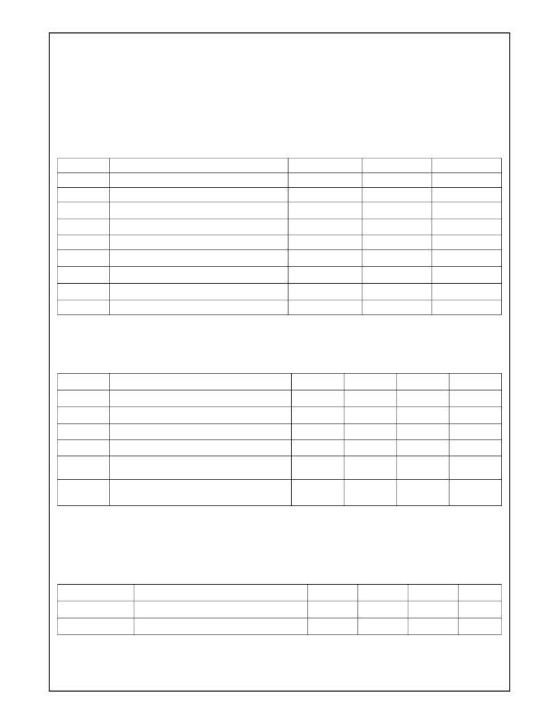
Table 9. Absolute Maximum Ratings
Symbol
Parameter
Min
Max
Unit
VCC
Core Logic Power Supply Voltage
-0.3
4.0
V
IOVCC
I/O Power Supply Voltage
-0.3
4.0
V
USB_VCC
1
USB Power Supply Voltage
-0.5
3.63
V
V
I
Voltage on any pad with GND = 0V
-0.5
3.6
V
PinRF
RF Input Power
+15
dBm
T
S
Storage Temperature Range
-65
+125
o
C
T
L
Lead Temperature (solder 4 sec)
+235
o
C
ESD-HBM
ESD, Human Body Model
2000
2
V
ESD-MM
ESD, Machine Model
200
V
1.
2.
USB Interface not supported by LMX9820A firmware. Treat as no connect. Pad required for mechanical stability.
Antenna pin passes 1500V HBM.
Table 10. Recommended Operating Conditions
1
Symbol
Parameter
Min
Typ
2
Max
Unit
VCC
3
Module Power Supply Voltage
2.85
3.3
3.6
V
IOVCC
4
I/O Power Supply Voltage
2.85
3.3
3.6
V
t
R
Module Power Supply Rise Time
50
ms
T
O
Operating Temperature Range
-40
+85
°C
HUM
OP
Humidity (operating, across operating
temperature range)
10
90
%
HUM
NONOP
Humidity (non-operating, 38.7
o
C web bulb
temperature)
5
95
%
1.
2.
3.
4.
Maximum voltage difference allowed between VCC and IOVCC is 500 mV.
Typical operating conditions are VCC = 3.3V, IOVCC = 3.3V operating voltage and 25°C ambient temperature.
VCC internally regulated to VDD_ANA (see Table 11)
IOVCC internally regulated to VDD_DIG (see Table 11)
Table 11. Power Supply Electrical Specifications (Analog and Digital LDOs)
Symbol
Parameter
Min
Typ
1
Max
Unit
VDD_ANA_OUT
2
Analog Voltage Output Range
2.8
V
VDD_DIG_OUT
3
Digital Voltage Output Range
2.5
V
1.
Typical operating conditions are VCC = 3.3V, IOVCC = 3.3V operating voltage and 25°C ambient temperature. Values
reflect voltages of internally generated, regulated voltages VDD_ANA and VDD_DIG
Output of internally generated regulated voltage VDD_ANA
Output of internally generated regulated voltage VDD_DIG
2.
3.
相關PDF資料 |
PDF描述 |
|---|---|
| LMX9820 | Bluetooth Serial Port Module |
| LMX9820SB | Bluetooth Serial Port Module |
| LMX9820SBX | Bluetooth Serial Port Module |
| LP3882ESX-1.2 | 1.5A Fast-Response Ultra Low Dropout Linear |
| LP3882ESX-1.5 | 1.5A Fast-Response Ultra Low Dropout Linear |
相關代理商/技術參數(shù) |
參數(shù)描述 |
|---|---|
| LMX9820ASM/NOPB | 制造商:Texas Instruments 功能描述:IC MODULE BLUETOOTH 116-LTCC |
| LMX9820ASMX | 制造商:NSC 制造商全稱:National Semiconductor 功能描述:Bluetooth Serial Port Module |
| LMX9820ASMX/NOPB | 制造商:Texas Instruments 功能描述:Bluetooth Class II 3.3V 0.704Mbps 116-Pin LTCC T/R 制造商:Texas Instruments 功能描述:MODULE BLUETOOTH SERIAL PORT SMD |
| LMX9820SB | 制造商:Texas Instruments 功能描述: 制造商:Texas Instruments 功能描述:MODULE BLUE TOOTH 116-LTCC 制造商:Texas Instruments 功能描述:BLUETOOTH MODULE 2.4GHZ 704KBPS |
| LMX9820SBX | 制造商:NSC 制造商全稱:National Semiconductor 功能描述:Bluetooth Serial Port Module |
發(fā)布緊急采購,3分鐘左右您將得到回復。