- 您現(xiàn)在的位置:買賣IC網(wǎng) > PDF目錄358887 > LMX2604LQ (NATIONAL SEMICONDUCTOR CORP) Triple-band VCO for GSM900/DCS1800/PCS1900 PDF資料下載
參數(shù)資料
| 型號: | LMX2604LQ |
| 廠商: | NATIONAL SEMICONDUCTOR CORP |
| 元件分類: | XO, clock |
| 英文描述: | Triple-band VCO for GSM900/DCS1800/PCS1900 |
| 中文描述: | VCO, 880 MHz - 915 MHz |
| 封裝: | LLP-20 |
| 文件頁數(shù): | 3/14頁 |
| 文件大小: | 268K |
| 代理商: | LMX2604LQ |
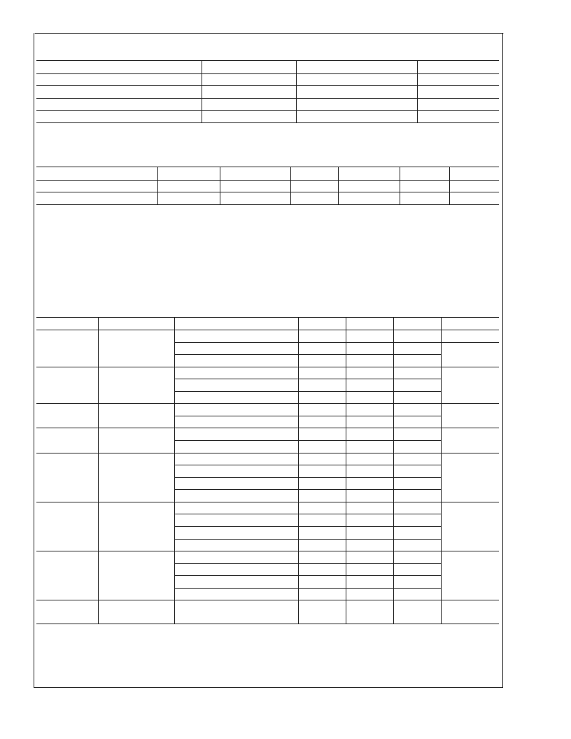
Absolute Maximum Ratings
(Notes 3, 4, 5)
Parameter
Symbol
V
DD
V
IN
I
IN
T
STG
Ratings
-0.3 to 3.6
-0.3 to V
DD
+0.3
10
-65 to 150
Unit
V
V
mA
C
Supply Voltage
Input Voltage
Input Current (Note 2)
Storage Temperature Range
Note 2:
Maximum input current is for a logic pin, not the power pins.
Recommended Operating Conditions
Parameter
Ambient Temperature
Supply Voltage (to GND)
Symbol
T
A
V
DD
Condition
V
DD
=3V
Min
-30
2.6
Typical
25
2.8
Max
85
3.0
Unit
C
V
Note 3:
“Absolute Maximum Ratings” indicate limits beyond which damage to the device may occur. Operating Ratings indicate conditions for which the device is
intended to be functional, but do not guarantee specific performance limits. For guaranteed specifications and test conditions, see the Electrical Characteristics. The
guaranteed specifications apply only for the test conditions listed.
Note 4:
This Device is a high performance RF integrated circuit with an ESD rating
<
2 kV and is ESD sensitive. Handling and assembly of this device should only
be done at ESD-free workstations.
Note 5:
Stresses in excess of the absolute maximum ratings can cause permanent or latent damage to the device. These are absolute stress ratings only.
Functional operation of the device is only implied at these or any other conditions in excess of those given in the operation sections of the data sheet. Exposure to
absolute maximum ratings for extended periods can adversely affect device reliability
Electrical Characteristics
AC Characteristics (V
DD
=2.8V, T
A
=25C; unless otherwise noted)
Symbol
Parameter
Remarks
GSM Band
DCS Band
PCS Band
GSM Band
DCS Band
PCS Band
GSM Band
DCS & PCS Band
GSM Band
DCS & PCS Band
at 100 kHz offset
at 400 kHz offset
at 3 MHz offset (Note 7)
at 20 MHz offset (Note 7)
at 100 kHz offset
at 400 kHz offset
at 3 MHz offset (Note 7)
at 20 MHz offset (Note 7)
at 100 kHz offset
at 400 kHz offset
at 3 MHz offset (Note 7)
at 20 MHz offset (Note 7)
Min
880
1710
1850
10
15
20
4
4
-5.5
-4.5
Typ
Max
915
1785
1910
20
25
30
8
8
-1.5
-0.5
Units
MHz
f
Frequency Range
MHz
K
VCO
Tuning Sensitivity
(Note 6)
15
20
25
6
6
-3.5
-2.5
-120
-136
-152
-167
-112
-130
-146
-163
-110
-129
-145
-162
MHz/V
Pout
Output Power
dBm
PMIXout
Output power of
MIXout pin
dBm
L(f)
Phase Noise
(GSM Band)
dBc/Hz
-128
L(f)
Phase Noise
(DCS Band)
dBc/Hz
-124
L(f)
Phase Noise
(PCS Band)
dBc/Hz
-124
Second Harmonic
Suppression
All Bands at RF output port.
-20
-15
dBc
Note 6:
Tuning Sensitivty is measured after coarse lock. Minimum and maximum limits are supported by characterization.
Note 7:
Supported by characterization
L
www.national.com
3
相關(guān)PDF資料 |
PDF描述 |
|---|---|
| LMX2604LQX | Triple-band VCO for GSM900/DCS1800/PCS1900 |
| LMX321 | Single/Dual/Quad, General-Purpose, Low-Voltage, Rail-to-Rail Output Op Amps |
| LMX321AXK-T | Single/Dual/Quad, General-Purpose, Low-Voltage, Rail-to-Rail Output Op Amps |
| LMX321AUK-T | Single/Dual/Quad, General-Purpose, Low-Voltage, Rail-to-Rail Output Op Amps |
| LMX321AXK | PLASTIC ENCAPSULATED DEVICES |
相關(guān)代理商/技術(shù)參數(shù) |
參數(shù)描述 |
|---|---|
| LMX2604LQX | 制造商:NSC 制造商全稱:National Semiconductor 功能描述:Triple-band VCO for GSM900/DCS1800/PCS1900 |
| LMX3120M | 制造商:未知廠家 制造商全稱:未知廠家 功能描述:Microwave/Millimeter Wave Amplifier |
| LMX3150TMX | 制造商:Rochester Electronics LLC 功能描述:- Bulk |
| LMX3160 | 制造商:NSC 制造商全稱:National Semiconductor 功能描述:Single Chip Radio Transceiver |
| LMX3161 | 制造商:NSC 制造商全稱:National Semiconductor 功能描述:Single Chip Radio Transceiver |
發(fā)布緊急采購,3分鐘左右您將得到回復(fù)。