- 您現(xiàn)在的位置:買賣IC網(wǎng) > PDF目錄358887 > LMX2525LQX1321 (NATIONAL SEMICONDUCTOR CORP) PLLatinum Dual Frequency Synthesizer System with Integrated VCOs PDF資料下載
參數(shù)資料
| 型號: | LMX2525LQX1321 |
| 廠商: | NATIONAL SEMICONDUCTOR CORP |
| 元件分類: | XO, clock |
| 英文描述: | PLLatinum Dual Frequency Synthesizer System with Integrated VCOs |
| 中文描述: | PLL FREQUENCY SYNTHESIZER, 26 MHz, QCC24 |
| 封裝: | 5 X 4 MM, 0.75 MM HEIGHT, LLP-24 |
| 文件頁數(shù): | 9/17頁 |
| 文件大?。?/td> | 237K |
| 代理商: | LMX2525LQX1321 |
Functional Description
GENERAL
The LMX2525 is a highly integrated frequency synthesizer
system for Japan PDC wireless communication systems.
The LMX2525 supports dual band operation for 800 MHz
and 1500 MHz.
The LMX2525 includes all functional blocks for the RF PLL
including RF VCOs, frequency dividers, PFDs, and loop
filters. Only external passive elements for the RF2 VCO tank
and supply bypassing are required to complete the RF syn-
thesizer.
The LMX2525 uses a patent pending Fractional-N synthe-
sizer architecture based on a delta sigma modulator to sup-
port fine frequency resolution. Four of the most common
reference frequencies for PDC applications, 12.6 MHz, 14.4
MHz, 25.2 MHz and 26.0 MHz, are supported. The unique
feature of this architecture is its low spurious modulation
effect.
The use of a fractional synthesizer based on a delta sigma
modulator allows for faster lock and system set-up times,
which reduces system power consumption. The loop filter is
included on chip to minimize the external noise coupling and
to reduce the form factor applicable to the board level appli-
cation. Only one of the two RF VCOs is activated at a given
time, and each output is provided through its own output pin.
RF PLL SECTION
Frequency Selection
The divide ratio can be calculated using the following equa-
tions:
f
VCO
= {8 x RF_B + RF_A+ (RF_FN / FD)} x (f
OSC
/ R) where
(RF_A
<
RF_B) for PDC1500
f
VCO
= {4 x RF_B + RF_A+ (RF_FN / FD)} x (f
OSC
/ R) where
(RF_A
<
RF_B) for PDC800
f
VCO
: Output frequency of voltage controlled oscillator (VCO)
RF_B: Preset divide ratio of binary 4-bit programmable
counter (2
≤
RF_B
≤
15)
RF_A: Preset divide ratio of binary 3-bit swallow counter (0
≤
RF_A
≤
7 for PDC1500 and 0
≤
RF_A
≤
3 for PDC800)
RF_FN: Preset numerator of binary 10-bit modulus counter
(0
≤
RF_FN
<
FD)
FD: Preset denominator for modulus counter (FD = f
OSC
/(R
X f
CH
) where f
CH
is the channel spacing)
f
OSC
: Reference oscillator frequency
R: Internal reference oscillator frequency divider (1 for 12.6
MHz and 14.4 MHz, 2 for 25.2 MHz and 26.0 MHz)
The denominator, FD, in the above equation is dependent on
the channel spacing and reference oscillator frequency. The
channel spacing will change based on the Rx/Tx and BS
bits.
Table 6
in the R0 Register section summarizes the
values of FD.
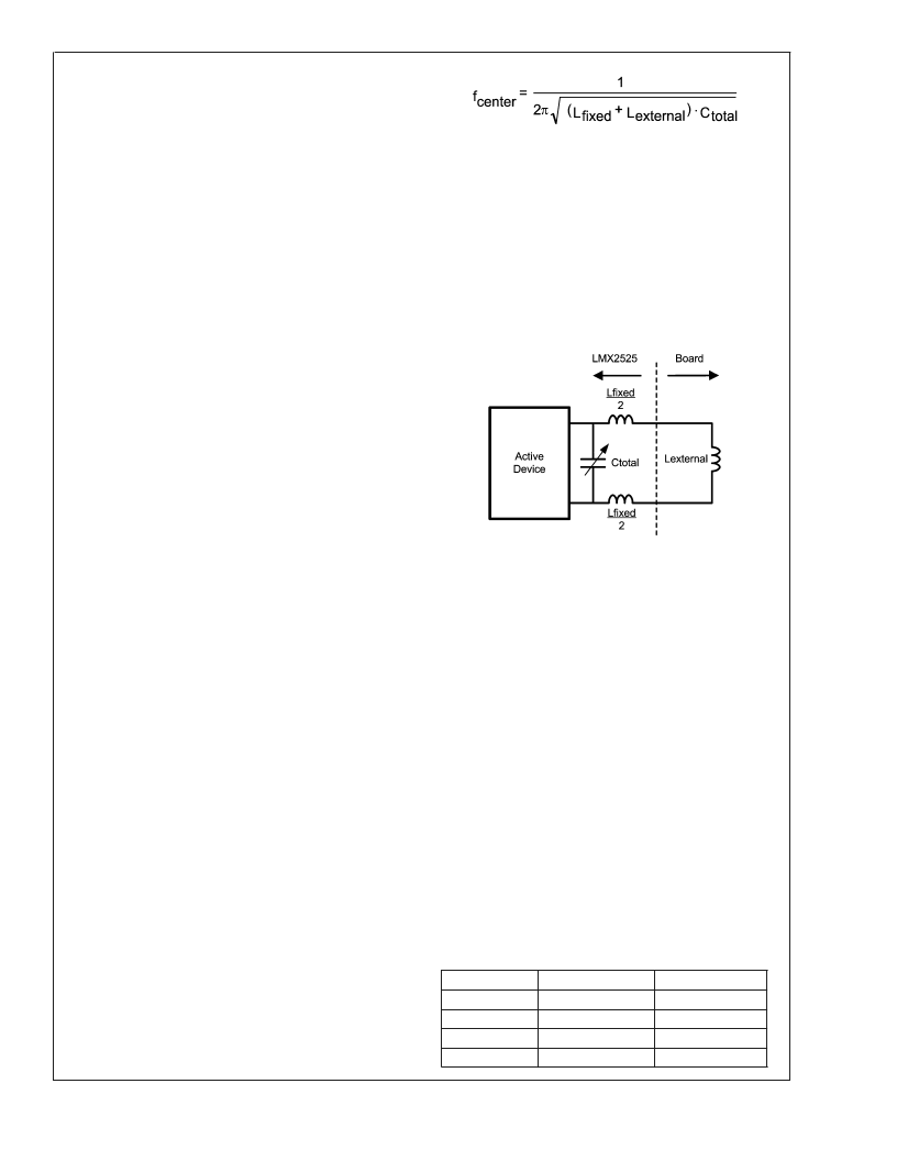
VCO Frequency Tuning
The center frequency of the RF VCOs are determined by the
resonant frequency of the tank circuit, illustrated in
Figure 1
.
With an internal fixed bonding-wire inductor and an external
inductance, the center frequency of the VCO is given as
follows:
20068910
where C
is the total capacitance of the VCO, including
the parasitic capacitance and the nominal self-tuning capaci-
tance. Note, the external inductance consists of the PCB
traces and lumped element inductor. The output frequency
tuning range can be optimized for the specific application by
selecting the appropriate external inductance. Refer to RF2
VCO Tuning Range vs. External Inductance plot to aid in
selecting the appropriate external inductance. Care should
be taken to ensure proper frequency coverage when choos-
ing the tolerance of the lumped element inductor. For the
1500 MHz band, the internal bonding-wires provide the nec-
essary inductance to set the VCO center frequency.
In real implementation, the inductance of L
and L
can vary from its nominal value. The LMX2525 utilizes a
built-in tracking algorithm to compensate for variations up to
±
15% and tunes the VCO to the required frequency. During
the frequency acquisition period, the loop bandwidth is ex-
tended to achieve the frequency lock. After the frequency
lock, the loop bandwidth of the PLL is set to the nominal
value and the phase lock is achieved. The transition be-
tween the two operating modes is very smooth and ex-
tremely fast to meet the stringent PDC requirements for lock
time and phase noise.
POWER DOWN MODE
The LMX2525 includes the power down mode to reduce the
power consumption. The LMX2525 enters the power down
mode either by taking the CE pin LOW or by setting the
RF_PD bit in the R0 register. If the CE pin is set LOW, the
circuit is powered down regardless of the register values.
When the CE pin is HIGH, the RF_PD bit controls power to
the RF circuitry. Data can be written to the registers even
when the CE pin is set LOW. The following truth table
summarizes the power down logic.
TABLE 1. Power Down Modes
CE Pin
HIGH
HIGH
LOW
LOW
RF_PD Bit
0
1
0
1
Mode
Active
Not Active
Not Active
Not Active
20068905
FIGURE 1. External Inductor Connection
L
www.national.com
9
相關(guān)PDF資料 |
PDF描述 |
|---|---|
| LMX2532LQ1065 | PLLatinum Frequency Synthesizer System with Integrated VCOs |
| LMX2532LQX0967 | PLLatinum Frequency Synthesizer System with Integrated VCOs |
| LMX2532LQX1065 | PLLatinum Frequency Synthesizer System with Integrated VCOs |
| LMX2532LQ0967 | PLLatinum Frequency Synthesizer System with Integrated VCOs |
| LMX2532 | PLLatinum Frequency Synthesizer System with Integrated VCOs |
相關(guān)代理商/技術(shù)參數(shù) |
參數(shù)描述 |
|---|---|
| LMX2525LQX1321/NOPB | 功能描述:IC FREQ SYNTH DUAL VCO 24-LLP RoHS:是 類別:RF/IF 和 RFID >> RF 其它 IC 和模塊 系列:PLLatinum™ 標準包裝:100 系列:* |
| LMX2531 | 制造商:NSC 制造商全稱:National Semiconductor 功能描述:High Performance Frequency Synthesizer System with Integrated VCO |
| LMX2531_07 | 制造商:NSC 制造商全稱:National Semiconductor 功能描述:High Performance Frequency Synthesizer System with Integrated VCO |
| LMX25311146EVAL | 功能描述:時鐘和定時器開發(fā)工具 LMX2531LQ1146 EVAL BOARD RoHS:否 制造商:Texas Instruments 產(chǎn)品:Evaluation Modules 類型:Clock Conditioners 工具用于評估:LMK04100B 頻率:122.8 MHz 工作電源電壓:3.3 V |
| LMX25311146EVAL/NOPB | 功能描述:射頻開發(fā)工具 LMX25311146 EVAL MOD RoHS:否 制造商:Taiyo Yuden 產(chǎn)品:Wireless Modules 類型:Wireless Audio 工具用于評估:WYSAAVDX7 頻率: 工作電源電壓:3.4 V to 5.5 V |
發(fā)布緊急采購,3分鐘左右您將得到回復。