- 您現(xiàn)在的位置:買賣IC網(wǎng) > PDF目錄361044 > LMX2434SLEX (NATIONAL SEMICONDUCTOR CORP) PLLatinum Dual High Frequency Synthesizer for RF Personal Communications PDF資料下載
參數(shù)資料
| 型號(hào): | LMX2434SLEX |
| 廠商: | NATIONAL SEMICONDUCTOR CORP |
| 元件分類: | XO, clock |
| 英文描述: | PLLatinum Dual High Frequency Synthesizer for RF Personal Communications |
| 中文描述: | PLL FREQUENCY SYNTHESIZER, 5000 MHz, PQCC20 |
| 封裝: | PLASTIC, UTCSP-20 |
| 文件頁(yè)數(shù): | 35/49頁(yè) |
| 文件大小: | 943K |
| 代理商: | LMX2434SLEX |
第1頁(yè)第2頁(yè)第3頁(yè)第4頁(yè)第5頁(yè)第6頁(yè)第7頁(yè)第8頁(yè)第9頁(yè)第10頁(yè)第11頁(yè)第12頁(yè)第13頁(yè)第14頁(yè)第15頁(yè)第16頁(yè)第17頁(yè)第18頁(yè)第19頁(yè)第20頁(yè)第21頁(yè)第22頁(yè)第23頁(yè)第24頁(yè)第25頁(yè)第26頁(yè)第27頁(yè)第28頁(yè)第29頁(yè)第30頁(yè)第31頁(yè)第32頁(yè)第33頁(yè)第34頁(yè)當(dāng)前第35頁(yè)第36頁(yè)第37頁(yè)第38頁(yè)第39頁(yè)第40頁(yè)第41頁(yè)第42頁(yè)第43頁(yè)第44頁(yè)第45頁(yè)第46頁(yè)第47頁(yè)第48頁(yè)第49頁(yè)
1.0 Functional Description
(Continued)
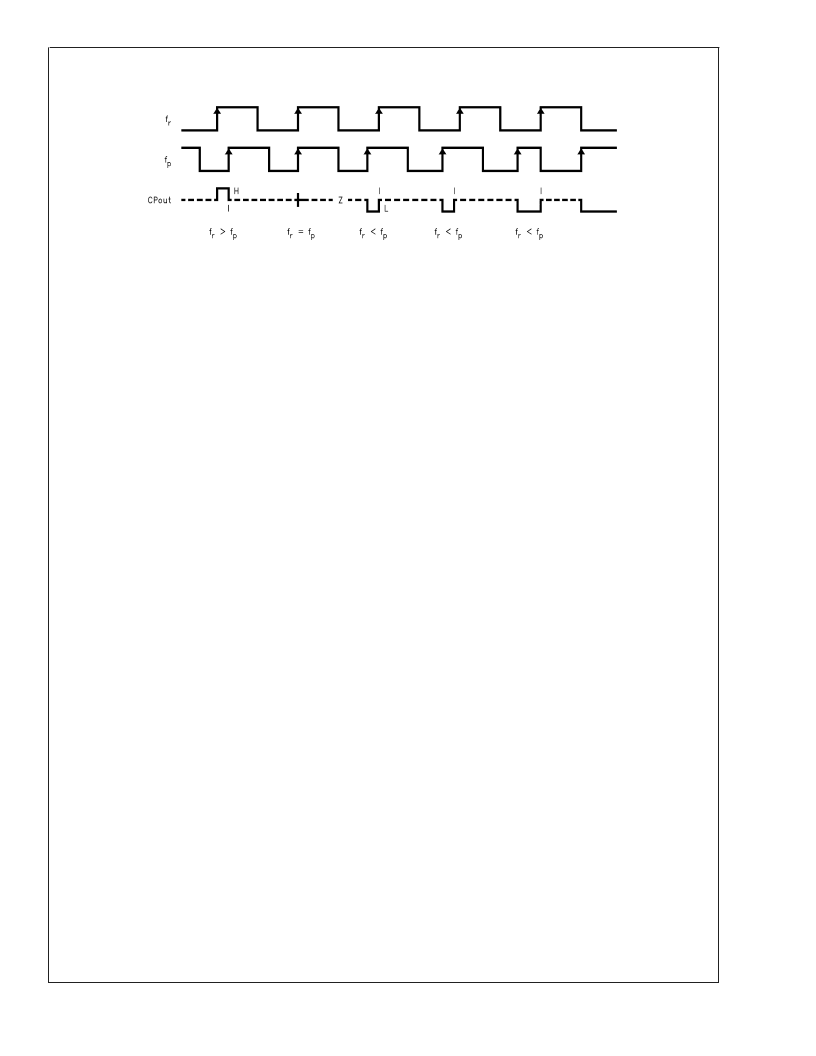
1.5.1 Phase Comparator and Internal Charge Pump Characteristics
20053511
Notes:
1.
2.
3.
4.
5.
The minimum width of the pump-up and pump-down current pulses occur at the CPoutRF or CPoutIF pins when the loop is phase locked.
The diagram assumes positive VCO characteristics, i.e. RF_CPP or IF_CPP = 1.
f
r
is the PFD input from the reference divider (R counter).
f
p
is the PFD input from the programmable feedback divder (N counter).
CPout refers to either the RF or IF charge pump output.
1.6 CHARGE PUMPS
The charge pump directs charge into or out of an external
loop filter. The loop filter converts the charge into a stable
control voltage which is applied to the tuning input of the
VCO. The charge pump steers the VCO control voltage
towards Vcc during pump-up events and towards GND dur-
ing pump-down events. When locked, CPoutRF or CPoutIF
are primarily in a TRI-STATE mode with small corrections
occuring at the phase comparator rate. The charge pump
output current magnitude can be selected by toggling the
RF_CPG
or
IF_CPG
control bits.
1.7 MICROWIRE SERIAL INTERFACE
The programmable register set is accessed via the MI-
CROWIRE serial interface. A low voltage logic interface
allows direct connection to 1.8V devices. The interface is
comprised of three signal pins: CLK, DATA and LE. Serial
data is clocked into the 24-bit shift register on the rising edge
of CLK. The last two bits decode the internal control register
address. When LE transitions HIGH, DATA stored in the shift
register is loaded into one of four control registers depending
on the state of the address bits. The MSB of DATA is loaded
in first. The synthesizers can be programmed even in power
down mode. A complete programming description is pro-
vided in
Section 2.0 Programming Description
.
1.8 MULTI-FUNCTION OUTPUTS
The LMX243x device’s Ftest/LD output pin is a multi-function
output that can be configured as a general purpose CMOS
TRI-STATE output, push-pull analog lock detect output,
open-drain analog lock detect output, digital filtered lock
detect output, or used to monitor the output of the various
reference divider (R counter) or feedback divider (N counter)
circuits. The Ftest/LD control word is used to select the
desired output function. When the PLL is in powerdown
mode, the Ftest/LD output is disabled and is in a high
impedance state.Acomplete programming description of the
multi-function output is provided in
Section 2.10
.
1.8.1 Push-Pull Analog Lock Detect Output
An analog lock detect status generated from the phase
detector is available on the Ftest/LD output pin if selected. A
push-pull configuration can be selected for the lock detect
output signal. With this configuration, the lock detect output
goes HIGH when the charge pump is inactive. It goes LOW
when the charge pump is active during a comparison cycle.
Narrow low going pulses are observed when the charge
pump turns on.
There are three separate push-pull analog lock detect sig-
nals that are routed to the multiplexer. Two of these monitor
the lock status of the individual synthesizers. The third de-
tects the condition when both the RF and IF synthesizers are
in a locked state. External circuitry is required to provide a
steady DC signal to indicate when the PLL is in a locked
state. Refer to
Section 2.10
for details on how to program
the different push-pull analog lock detect options.
1.8.2 Open-Drain Analog Lock Detect Output
The lock detect output can be an open-drain configuration. In
this configuration, the lock detect output goes to a high
impedance state when the charge pump is inactive. It goes
LOW when the charge pump is active during a comparison
cycle. When a pull-up resistor is used, narrow low going
pulses are observed when the charge pump turns on.
Similarly, three separate open-drain analog lock detect sig-
nals are routed to the multiplexer. Two of these monitor the
lock status of the individual synthesizers. The third detects
the condition when both the RF and IF synthesizers are in a
locked state. External circuitry is required to provide a steady
DC signal to indicate when the PLL is in a locked state. Refer
to
Section 2.10
for details on how to program the different
open-drain analog lock detect options.
L
www.national.com
35
相關(guān)PDF資料 |
PDF描述 |
|---|---|
| LMX2531LQ1570E | PLLatinum High Performance Frequency Synthesizer System with Integrated VCO |
| LMX2531 | PLLatinum High Performance Frequency Synthesizer System with Integrated VCO |
| LMX2531LQ1650E | PLLatinum High Performance Frequency Synthesizer System with Integrated VCO |
| LMX2531LQ1778E | PLLatinum High Performance Frequency Synthesizer System with Integrated VCO |
| LMX2531LQ2080E | PLLatinum High Performance Frequency Synthesizer System with Integrated VCO |
相關(guān)代理商/技術(shù)參數(shù) |
參數(shù)描述 |
|---|---|
| LMX2434SLEX/NOPB | 功能描述:鎖相環(huán) - PLL RoHS:否 制造商:Silicon Labs 類型:PLL Clock Multiplier 電路數(shù)量:1 最大輸入頻率:710 MHz 最小輸入頻率:0.002 MHz 輸出頻率范圍:0.002 MHz to 808 MHz 電源電壓-最大:3.63 V 電源電壓-最小:1.71 V 最大工作溫度:+ 85 C 最小工作溫度:- 40 C 封裝 / 箱體:QFN-36 封裝:Tray |
| LMX2434TM | 制造商:Texas Instruments 功能描述:PLL Frequency Synthesizer Dual 500MHz to 5000MHz 20-Pin TSSOP Rail |
| LMX2434TM/NOPB | 功能描述:鎖相環(huán) - PLL 5.0Ghz High Freq Dual Pll RoHS:否 制造商:Silicon Labs 類型:PLL Clock Multiplier 電路數(shù)量:1 最大輸入頻率:710 MHz 最小輸入頻率:0.002 MHz 輸出頻率范圍:0.002 MHz to 808 MHz 電源電壓-最大:3.63 V 電源電壓-最小:1.71 V 最大工作溫度:+ 85 C 最小工作溫度:- 40 C 封裝 / 箱體:QFN-36 封裝:Tray |
| LMX2434TMX | 功能描述:鎖相環(huán) - PLL RoHS:否 制造商:Silicon Labs 類型:PLL Clock Multiplier 電路數(shù)量:1 最大輸入頻率:710 MHz 最小輸入頻率:0.002 MHz 輸出頻率范圍:0.002 MHz to 808 MHz 電源電壓-最大:3.63 V 電源電壓-最小:1.71 V 最大工作溫度:+ 85 C 最小工作溫度:- 40 C 封裝 / 箱體:QFN-36 封裝:Tray |
| LMX2434TMX/NOPB | 功能描述:鎖相環(huán) - PLL RoHS:否 制造商:Silicon Labs 類型:PLL Clock Multiplier 電路數(shù)量:1 最大輸入頻率:710 MHz 最小輸入頻率:0.002 MHz 輸出頻率范圍:0.002 MHz to 808 MHz 電源電壓-最大:3.63 V 電源電壓-最小:1.71 V 最大工作溫度:+ 85 C 最小工作溫度:- 40 C 封裝 / 箱體:QFN-36 封裝:Tray |
發(fā)布緊急采購(gòu),3分鐘左右您將得到回復(fù)。