- 您現(xiàn)在的位置:買賣IC網(wǎng) > PDF目錄361042 > LMV115MGX (NATIONAL SEMICONDUCTOR CORP) TRANS PNP HF 60VCEO 2A TO-126 PDF資料下載
參數(shù)資料
| 型號: | LMV115MGX |
| 廠商: | NATIONAL SEMICONDUCTOR CORP |
| 元件分類: | 運(yùn)動(dòng)控制電子 |
| 英文描述: | TRANS PNP HF 60VCEO 2A TO-126 |
| 中文描述: | BUFFER AMPLIFIER, PDSO6 |
| 封裝: | 2.10 X 2 MM, SC-70, 6 PIN |
| 文件頁數(shù): | 10/13頁 |
| 文件大小: | 475K |
| 代理商: | LMV115MGX |
Application Section
GENERAL
The LMV115 is specially designed to minimize the effects of
spurious signals from the base band chip to the oscillator.
Beside this the influence of varying load resistance and
capacitance to the oscillator is minimized, while increasing
the drive capability. The input of the LMV115 is internally
biased with two equal resistors to the power supply rails, and
makes AC coupling possible without external bias resistors
at the input. The LMV115 has excellent gain phase margin.
The LMV115 offers a shutdown pin that can be used to
disable the device in order to optimize current consumption
and also has a feature to control the supply voltage to an
external oscillator. When the shutdown pin is connected to
V
DD
the device is in shutdown mode.
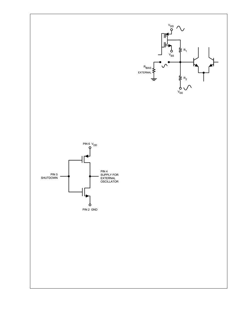
SWITCHED POWER SUPPLY CONNECTION
The LMV115 features an enable/disable function for an ex-
ternal oscillator by controlling its supply voltage (pin 4). See
also the schematic diagram on the front page. During normal
operating mode, pin 4 is connected to the positive supply rail
via an internal switch. The resistance between the positive
supply rail and pin 4, R
, is specified in the electrical
characterization table. Oscillators with a supply current up to
several milliamps can easily be powered from pin 4. During
shutdown, pin 4 is switched to the negative supply rail. The
simplified schematic for this part of the device is shown in
Figure 1
INPUT CONFIGURATION
The input of the LMV115 is internally biased at mid-supply by
a divider of two equal resistors. With the LMV115 in shut-
down mode, the internal resistor connected to the V
is
shortened to the negative power supply rail via a switch. This
makes the power consumption in ‘off’ mode almost zero, but
causes a small difference for the input impedance between
the on and off modes. Both resistors are 110k
so the
resulting input impedance will be approximately 55k
. The
input configuration allows AC coupling on the input of the
LMV115. A simplified schematic of the input is shown in
Figure 2
.
PSRR
If an AC signal is applied to one of the supply lines, while the
input is floating, the signal at the input pin is half the signal at
the supply line, causing the same signal at the output of the
buffer. This will result in a PSRR of only 6dB (see
Figure 2
).
In a typical application the input is driven from a low ohmic
source that means the disturbance at the supply lines is
attenuated by the series resistors of 110k and the source
impedance. In case the buffer is connected to a 50
source,
the resulting suppression will be 20*log [(R
+ R
)/R
]
= 67dB for signals at the supply line. The PSRR can also be
measured correctly for this type of input by shorten the input
to mid-supply. Due to the internal structure it is not recom-
mended to measure with the input connected to ground. To
measure correctly the PSRR, two signals are applied to both
V
and V
but with 180 phase difference (see
Figure 2
).
In this case, both signals are subtracted and there will be no
signal at the input. The resulting disturbance at the output is
now only caused by the signals at the supply lines.
INPUT AND OUTPUT LEVEL
Due to the internal loop gain of 1, the output will follow the
input. The output voltage cannot swing as close to the supply
rail as the input voltage. For linear operation the input volt-
age swing should not exceed the output voltage swing. The
restrictions for the output voltage can be examined by the
two curves in
Figure 3
. The curve V
OUT
(V) shows the
response of the output signal versus the input signal and the
curve V
OUT
– V
IN
(V) shows the difference between the
output and the input signal.
20075131
FIGURE 1. Supply For External Oscillator
20075132
FIGURE 2. Dual Supply Mode
L
www.national.com
10
相關(guān)PDF資料 |
PDF描述 |
|---|---|
| LMV228TLX | RF Power Detector for CDMA and WCDMA |
| LMV225SD | RF Power Detector for CDMA and WCDMA |
| LMV225SDX | RF Power Detector for CDMA and WCDMA |
| LMV225TL | RF Power Detector for CDMA and WCDMA |
| LMV225TLX | RF Power Detector for CDMA and WCDMA |
相關(guān)代理商/技術(shù)參數(shù) |
參數(shù)描述 |
|---|---|
| LMV115MGX/NOPB | 功能描述:IC CLOCK BUFFER SGL 30MHZ SC70-6 RoHS:是 類別:RF/IF 和 RFID >> RF 其它 IC 和模塊 系列:- 標(biāo)準(zhǔn)包裝:100 系列:* |
| LMV116 | 制造商:NSC 制造商全稱:National Semiconductor 功能描述:Low Voltage, 45MHz, Rail-to-Rail Output Operational Amplifiers with Shutdown Option |
| LMV116MF | 功能描述:運(yùn)算放大器 - 運(yùn)放 RoHS:否 制造商:STMicroelectronics 通道數(shù)量:4 共模抑制比(最小值):63 dB 輸入補(bǔ)償電壓:1 mV 輸入偏流(最大值):10 pA 工作電源電壓:2.7 V to 5.5 V 安裝風(fēng)格:SMD/SMT 封裝 / 箱體:QFN-16 轉(zhuǎn)換速度:0.89 V/us 關(guān)閉:No 輸出電流:55 mA 最大工作溫度:+ 125 C 封裝:Reel |
| LMV116MF/NOPB | 功能描述:運(yùn)算放大器 - 運(yùn)放 Sgl Mid-Speed RRO Op amp RoHS:否 制造商:STMicroelectronics 通道數(shù)量:4 共模抑制比(最小值):63 dB 輸入補(bǔ)償電壓:1 mV 輸入偏流(最大值):10 pA 工作電源電壓:2.7 V to 5.5 V 安裝風(fēng)格:SMD/SMT 封裝 / 箱體:QFN-16 轉(zhuǎn)換速度:0.89 V/us 關(guān)閉:No 輸出電流:55 mA 最大工作溫度:+ 125 C 封裝:Reel |
| LMV116MFX | 功能描述:運(yùn)算放大器 - 運(yùn)放 RoHS:否 制造商:STMicroelectronics 通道數(shù)量:4 共模抑制比(最小值):63 dB 輸入補(bǔ)償電壓:1 mV 輸入偏流(最大值):10 pA 工作電源電壓:2.7 V to 5.5 V 安裝風(fēng)格:SMD/SMT 封裝 / 箱體:QFN-16 轉(zhuǎn)換速度:0.89 V/us 關(guān)閉:No 輸出電流:55 mA 最大工作溫度:+ 125 C 封裝:Reel |
發(fā)布緊急采購,3分鐘左右您將得到回復(fù)。