- 您現(xiàn)在的位置:買賣IC網(wǎng) > PDF目錄367571 > LMS5213M7X-2.8 THREE-TERMINAL POSITIVE FIXED VOLTAGE REGULATORS PDF資料下載
參數(shù)資料
| 型號: | LMS5213M7X-2.8 |
| 元件分類: | 基準(zhǔn)電壓源/電流源 |
| 英文描述: | THREE-TERMINAL POSITIVE FIXED VOLTAGE REGULATORS |
| 中文描述: | 三端固定電壓調(diào)節(jié)器 |
| 文件頁數(shù): | 3/8頁 |
| 文件大小: | 221K |
| 代理商: | LMS5213M7X-2.8 |

Absolute Maximum Ratings
(Note 1)
If Military/Aerospace specified devices are required,
please contact the National Semiconductor Sales Office/
Distributors for availability and specifications.
ESD Tolerance (Note 2)
Human Body Model
Junction Temperature
V
IN
, V
OUT
, V
EN
Soldering Information
Infrared or Convection (20 sec)
Wave Soldering (10 sec)
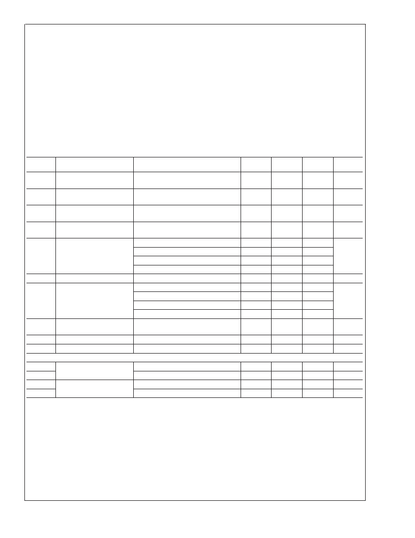
Electrical Characteristics
Unless otherwise specified, all limits guaranteed for T
J
= 25C, V
IN
= V
OUT
+ 1V, I
L
= 1mA, C
L
= 0.47μF, V
EN
≥
2.0V.
Bold-
face
limits apply at the temperature extremes.
Symbol
Parameter
Conditions
2000V
150C
0.3 TO 6.5V
235C
260C (lead temp)
Operating Ratings
Supply Voltages
V
IN
V
EN
Junction Temp. Range (Note 3)
Storage Temperature Range
Package Themal Resistance
SC70-5
2.7V to 6V
0V to V
IN
40C to +125C
65C to 150C
478C/W
Min
(Note 5)
-3
-4
Typ
(Note 4)
Max
(Note 5)
3
4
200
Units
V
O
Output Voltage Accuracy
%
V
O
/
T
Output Voltage Temp.
Coefficient
Line Regulation
(Note 10)
50
ppm/C
V
O
/V
O
V
IN
= V
OUT
+1V to 6V
0.008
0.3
0.5
0.3
0.5
%
V
O
/V
O
Load Regulation
I
L
= 0.1mA to 80mA (Note 6)
0.08
%
V
IN
-V
O
Dropout Voltage
(Note 7)
I
L
= 100μA
I
L
= 20mA
I
L
= 50mA
I
L
= 80mA
V
EN
≤
0.4V (Shutdown)
I
L
= 100μA, V
EN
≥
2.0V (active)
I
L
= 20mA, V
EN
≥
2.0V (active)
I
L
= 50mA, V
EN
≥
2.0V (active)
I
L
= 80mA, V
EN
≥
2.0V (active)
V
IN
= V
OUT(NOMINAL)
–0.5V
20
70
180
330
1
160
180
200
220
200
mV
350
600
10
I
Q
I
GND
Quiescent Current
Ground Pin Current
μA
μA
750
3000
300
I
GNDDO
Ground Pin Current at
Dropout, (Note 8)
Current Limit
Thermal Regulation
μA
I
LIMIT
V
O
/
P
D
Enable Input
V
IL
V
IH
I
IL
I
IH
V
OUT
= 0V
(Note 9)
180
0.05
250
mA
%W
Enable Input Voltage Level
Logic Low (off)
Logic High (on)
V
IL
≤
0.6V
V
IH
≥
2.0V
0.6
V
V
μA
μA
2.0
Enable Input Current
0.01
15
1
50
Note 1:
Absolute Maximum Ratings indicate limits beyond which damage to the device may occur. Operating Ratings indicate conditions for which the device is
intended to be functional, but specific performance is not guaranteed. For guaranteed specifications and the test conditions, see the Electrical Characteristics.
Note 2:
Human body model, 1.5k
in series with 100pF.
Note 3:
The maximum power dissipation is a function of T
J(max)
,
θ
JA
, and T
A
. The maximum allowable power dissipation at any ambient temperature
is P
D
= (T
J(max)
–T
A
)/
θ
JA
. All numbers apply for packages soldered directly into a PC board.
Note 4:
Typical Values represent the most likely parametric norm.
Note 5:
All limits are guaranteed by testing or statistical analysis.
Note 6:
Regulation is measured at constant junction temperature using low duty cycle pulse testing. Changes in output voltage due to heating effects are covered
by the thermal regulation specification.
Note 7:
Dropout voltage is defined as the input to output differential at which the output voltage drops 2% below its nominal value measured at 1V differential.
Note 8:
Ground pin current is the regulator quiescent current plus pass transistor base current. The total current drawn from the supply is the sum of the load current
plus the ground pin current.
Note 9:
Thermal regulation is defined as the change in output voltage at a time “t” after a change in power dissipation is applied, excluding load or line regulation
effects. Specifications are for an 80mA load pulse at V
IN
= 6V for t = 16ms.
L
www.national.com
3
相關(guān)PDF資料 |
PDF描述 |
|---|---|
| LMU08CC35 | Multiplier |
| LMU08CC50 | Multiplier |
| LMU08CC70 | Multiplier |
| LMU08CM45 | Multiplier |
| LMU08CM60 | Multiplier |
相關(guān)代理商/技術(shù)參數(shù) |
參數(shù)描述 |
|---|---|
| LMS5214 | 制造商:NSC 制造商全稱:National Semiconductor 功能描述:80mA, Low Dropout Voltage Regulator with Auto Discharge Function in SC70 |
| LMS5214A-2.5 EA WAF | 制造商:Texas Instruments 功能描述: |
| LMS5214A-2.9 WAF | 制造商:Texas Instruments 功能描述: |
| LMS5214A-3.0 WAF | 制造商:Texas Instruments 功能描述: |
| LMS5214B-2.8 WAF | 制造商:Texas Instruments 功能描述: |
發(fā)布緊急采購,3分鐘左右您將得到回復(fù)。